Page 40 - Chip Scale Review_November December_2021-digital
P. 40
it has potential to fulfill diverse roles in
        interconnect applications. The material
        has, for example, been considered as
        an oxidation barrier and as an ultrathin
        diffusion barrier for metals. Researchers
        have also investigated the feasibility
        of using multilayer graphene wires or
        nanoribbons as an alternative conductor.
          Graphene, however, comes with one
        major drawback: intrinsically, it does
        not hold enough charge carriers to be
        useful as a local interconnect. The lack
        of charge carriers severely reduces its
        electrical conductivity—a key metric
        for interconnect performance that is
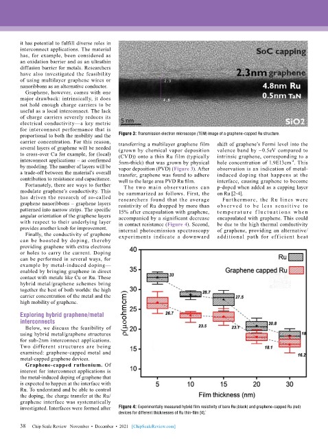
        proportional to both the mobility and the   Figure 3: Transmission electron microscope (TEM) image of a graphene-capped Ru structure.
        carrier concentration. For this reason,   transferring a multilayer graphene film   shift of graphene’s Fermi level into the
        several layers of graphene will be needed   (grown by chemical vapor deposition   valence band by ~0.5eV compared to
        to cross-over Cu for example, for (local)   (CVD)) onto a thin Ru film (typically   intrinsic graphene, corresponding to a
        interconnect applications – as confirmed   5nm-thick) that was grown by physical   hole concentration of 1.9E13cm . This
                                                                                                         -2
        by modeling. The number of layers will be   vapor deposition (PVD) (Figure 3). After   observation is an indication of metal-
        a trade-off between the material’s overall   transfer, graphene was found to adhere   induced doping that happens at the
        contribution to resistance and capacitance.  well to the large area PVD Ru film.  interface, causing graphene to become
          Fortunately, there are ways to further   The two main observations can   p-doped when added as a capping layer
        modulate graphene’s conductivity. This   be summarized as follows. First, the   on Ru [2-4].
        has driven the research of so-called   researchers found that the average   Furthermore, the Ru lines were
        graphene nanoribbons – graphene layers   resistivity of Ru dropped by more than   obser ved to be less sensit ive to
        patterned into narrow strips. The specific   15% after encapsulation with graphene,   t e m p e r a t u r e  f l u c t u a t ion s  w h e n
        angular orientation of the graphene layers   accompanied by a significant decrease   encapsulated with graphene. This could
        with respect to their underlying layer   in contact resistance (Figure 4). Second,   be due to the high thermal conductivity
        provides another knob for improvement.   internal photoemission spectroscopy   of graphene, providing an alternative/
          Finally, the conductivity of graphene   experiments indicate a downward   additional path for eff icient heat
        can be boosted by doping, thereby
        providing graphene with extra electrons
        or holes to carry the current. Doping
        can be performed in several ways, for
        example by metal-induced doping—
        enabled by bringing graphene in direct
        contact with metals like Cu or Ru. These
        hybrid metal/graphene schemes bring
        together the best of both worlds: the high
        carrier concentration of the metal and the
        high mobility of graphene.

        Exploring hybrid graphene/metal
        interconnects
          Below, we discuss the feasibility of
        using hybrid metal/graphene structures
        for sub-2nm interconnect applications.
        Two different structures are being
        examined: graphene-capped metal and
        metal-capped graphene devices.
          Graphene-capped ruthenium. Of
        interest for interconnect applications is
        the metal-induced doping of graphene that
        is expected to happen at the interface with
        Ru. To understand and be able to control
        the doping, the charge transfer at the Ru/
        graphene interface was systematically
        investigated. Interfaces were formed after   Figure 4: Experimentally measured hybrid film resistivity of bare Ru (black) and graphene-capped Ru (red)
                                           devices for different thicknesses of Ru thin-film [4].`

        38   Chip Scale Review   November  •  December  •  2021   [ChipScaleReview.com]
        38

