Page 40 - ChipScale_Jan-Feb_2020-digital
P. 40
Where are we with HDAP LVS verification?


        By Tarek Ramadan [Mentor, a Siemens Business]
        H          ig h - de n sit y a dva nce d


                   p a c k a g i ng ( H D A P )
                   c o m bi n e s  m u l t i p l e
        integrated circuit (IC) dies in a single
        package. This heterogeneous integration
        provides an improved form factor and
        enhanced functionality when compared to
        other packaging technologies, but presents
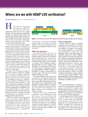
        some tricky verification challenges,   Figure 1: 2.5D interposer-based and FOWLP designs are the HDAP technologies currently used most frequently.
        because each of those die may be built   verification—using the two HDAP   Process ownership
        using a different technology node.   designs that are currently the most   Because HDAP is still an emerging
          Like any electronic product, HDAP   popular: 2.5D (interposer) and fan-out   technology, the responsibility for HDAP
        designs require extensive verification to   wafer-level packaging (FOWLP), shown   verification can vary from team to team
        ensure they will perform as intended, and   in Figure 1.              and company to company. For example,
        can be reliably manufactured in sufficient                            some design companies see 2.5D design
        quantities to meet market demand. Unlike   HDAP LVS verification      and verification as a “more SoC, less
        traditional ICs, system-on-chips (SoCs),   We all know that an SoC can’t be   packaging” activity, and assign design and
        or printed circuit boards (PCBs), however,   submitted to manufacturing unless the   verification tasks to SoC and/or computer-
        automating HDAP verification requires   geometries that are present in the physical   aided design (CAD) teams experienced in
        combining elements of both IC and   layout implement the connectivity   SoC verification requirements and formats,
        package verification. This has proved to be   and circuit performance created in the   but with limited packaging experience.
        somewhat challenging for the electronic   schematic/design intent. LVS verification   FOWLP design and verification, on the
        design automation (EDA) industry, though   is a mature, well-established, highly-  other hand, is viewed as a “less SoC, more
        it has invested a significant amount of   automated flow in the SoC design world.   packaging” activity, so responsibility
        time and research into categorizing the   To support the automated LVS process,   often goes to a packaging team that
        issues and developing solutions, and   LVS tools require a consistent set of data:   is less familiar with SoC verification
        progress is being made.            1) Layout database (GDSII, OASIS, or   requirements and formats. The bottom
          To begin with, the general concept of   LEF/DEF); 2) Source netlist (SPICE or   line is that foundries, OSATS, and EDA
        qualified assembly design kits (ADKs)   Verilog); and 3) LVS rule deck (format   companies cannot impose a single, uniform
        that are similar to foundry-qualified   depends on EDA tool used).    set of processes and conditions when
        process design kits (PDKs) for ICs [1-  The layout database and source netlist   supporting HDAP design companies using
        3] has become at least a limited reality   are created by the design company for   diverse methodologies and requirements.
        [4]. Assembly-level layout vs. schematic   each SoC design, while the LVS rules   Flexibility is essential to success.
        (LVS) verification for HDAPs [5-6] now   deck is typically created and provided by
        has at least one EDA solution [7]. The   the foundry, and is independent of any   Data
        value of post-layout simulation for analog   single SoC. Design companies, foundries,   To run full-package LVS verification,
        and post-layout static timing analysis   and EDA suppliers all understand and   all the data for all the HDAP components
        (STA) for digital flows for HDAPs is now   agree that SoC LVS verification can’t   must be available. For example, in a
        well-understood [8], as is the need for   happen without some combination of   FOWLP design, designers require: 1) Die1
        an automated approach that generates   these three inputs.            through Dien layout design databases; 2)
        HDAP system-level connectivity while   When we start to look at HDAP LVS   FOWLP design database; and 3) FOWLP
        accounting for die, package, and die/  verification, we immediately see major   system source netlist (in some form).
        package interface parasitics [9].  differences. The most obvious and    So what happens if the FOWLP design
          While the maturity and scope of the   most critical is that design companies,   database (owned by the packaging
        processes needed to make HDAPs a   foundries, outsourced assembly and test   team) is ready, while the individual
        viable market option may still be in   suppliers (OSATS), and EDA suppliers   die  databases  (owned  by  the  SoC
        development, this seems a good time   are neither in alignment, nor agreement,   teams) are still being developed? If the
        to assess where we are. To get an idea   on the set of inputs required for an HDAP   FOWLP designer has to wait until all
        of how far we’ve come, and where we   LVS flow. This disconnect exists for three   the dies are built and verified to run
        need to go, let’s take a closer look at   reasons: ownership, data availability, and   the FOWLP LVS and find out that the
        one particular process—package LVS   design dependence.               FOWLP design database is full of shorts,


        38   Chip Scale Review   January  •  February  •  2020   [ChipScaleReview.com]
        38

