Page 37 - ChipScale_Jan-Feb_2020-digital
P. 37
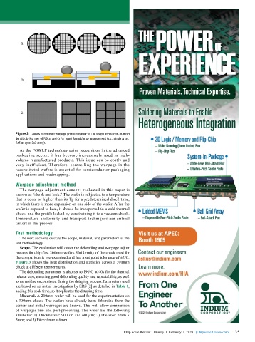
Figure 2: Causes of different warpage profile behavior: a) Die shape and silicon-to-mold
        density; b) Number of RDLs; and c) For panel format/array arrangement (e.g., single array,
        2x2 array or 3x3 array).
          As the FOWLP technology gains recognition in the advanced
        packaging sector, it has become increasingly used in high-
        volume manufactured products. This issue can be costly and
        very inefficient. Therefore, controlling the warpage in the
        reconstituted wafers is essential for semiconductor packaging
        applications and roadmapping.

        Warpage adjustment method
          The warpage adjustment concept evaluated in this paper is
        known as “shock and lock.” The wafer is subjected to a temperature
        that is equal or higher than its Tg for a predetermined dwell time,
        in which there is more expansion on one side of the wafer. After the
        wafer is exposed to heat, it should be transported to a cold thermal
        chuck, and the profile locked by constraining it to a vacuum chuck.
        Temperature uniformity and transport techniques are critical
        factors in this process.

        Test methodology
          The next sections discuss the scope, material, and parameters of the
        test methodology.
          Scope. The evaluation will cover the debonding and warpage adjust
        process for chip-first 200mm wafers. Uniformity of the chuck used for
        the comparison is pre-examined and has a set point tolerance of ±2ºC.
        Figure 3 shows the heat distribution and statistics across a 300mm
        chuck at different temperatures.
          The debonding parameter is also set to 190ºC at 40s for the thermal
        release tape, ensuring good debonding quality and repeatability, as well
        as no residue encountered during the detaping process. Parameters used
        are based on an initial investigation by ERS [2] as detailed in Table 1,
        adding 20s soak time, so it replicates the detaping time.
          Material. A 200mm wafer will be used for the experimentation on
        a 300mm chuck. The wafers have already been debonded from the
        carrier and initial warpages are known. This will allow comparison
        of warpages pre- and post-processing. The wafer has the following
        attributes: 1) Thicknesses: 900µm and 600µm; 2) Die size: 5mm x
        5mm; and 3) Pitch: 6mm x 6mm.

                                                                                                             35
                                                          Chip Scale Review   January  •  February  •  2020   [ChipScaleReview.com]  35

