Page 33 - ChipScale_Jan-Feb_2020-digital
P. 33
case of the spring elements examined   produce a surface that is as flat as possible.
        here, the double-acting structures   A scanning electron microscopy (SEM)
        proved to be advantageous on account   image of a closed cavity made by LIDE is
        of their structure and likely due to the   shown in Figure 10. The sidewalls have a
        spring force, which is approximately   taper angle of approximately 1º.
        twice as great in comparison with the   The advantages of using a capping
        other designs.                     wafer manufactured by LIDE for WLP
                                           essentially result from the favorable cross-
        Glass wafer-level packaging        section profile. This profile fits better to
        enabled by LIDE of closed cavities   the rectangular silicon dies and enables
          The following sections demonstrate how   higher population densities as it can be
        LIDE technology can manfacture closed   seen in the comparison between Figure 9
        pockets for glass capping wafers without   and Figure 11.
        having the drawback of under etching,
        which is usually associated with mask
        isotropic wet etching.
          WLP with glass capping wafer. Wafer-
        level packaging (WLP) is an established
        low-cost and high-volume production                                   Figure 14: Light microscopy image of a cross
                                                                              section of a cavity made by LIDE.
        technology [5]. Glass capping wafers are
        usually made with an etch mask (typically                             of the closed cavities with different
        chromium) and subsequently wet etched.   Figure 11: Schematic of wafer-level packaging with   roughnesses. Roughness measurements of
        This process is associated with under   a LIDE-processed glass capping wafer.  the bottom of the cavities will be addressed
        etching of the etch mask, resulting in                                later in the measurement results paragraph
        capping wafers with closed cavities that   Variation of pitch between laser-  where we will show that a longer etching
        have a pronounced fillet at the bottom and   induced modifications. The roughness   time leads to a better bottom cavity
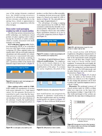
        limited to aspect-ratios below 1 (Figure 9).   of the cavity mainly depends on the   roughness. To measure the cavity depth, the
                                           distance between the individual laser   glass panel was cut with a diamond scribing
                                           modifications of the glass. To evaluate   wheel. The cutting facet was then inspected
                                           the cavity roughness, the pitch of the   with a Keyence VK X210 microscope and
                                                                              the glass thickness and cavity depth were
                                                                              measured (see Figure 14).
                                                                                As it is shown in Figure 15, if etched
                                                                              longer, the spikes at the bottom of the
                                                                              cavities are reduced, as is the roughness.
                                                                              So, the etching time parameter can be used
        Figure 9: Schematic of wafer-level packaging with
        a standard glass capping wafer.                                       to achieve the requested roughness down to
                                                                              a Ra of ≈ 0.5µm.
          Glass capping wafers made by LIDE.                                    Discussion. The positional accuracy of
        LIDE enables the manufacture of cavities                              closed cavities made by LIDE is within
        with steep sidewalls (i.e., high aspect   Figure 12: Schematic of the cavity shown in Figure 11.  what was expected, as the laser tool
        ratios). For this purpose, the process is                             specification is within +/-5µm (Cpk>1.33).
        controlled in such a way that the laser-  laser modifications was progressively   The width and height of the cavities are
        induced modifications are intentionally   changed. A schematic visualization of   defined by the same direct writing process.
        not introduced over the entire thickness of   the laser modifications and the resulting
        the substrate. Usually, the modifications   etched profile are shown in Figure 12.
        are arranged in a hexagonal pattern to   Figure 13 shows different SEM pictures


                                                                              Figure 15: Measurement results of the roughness
                                                                              of the bottom cavities versus the laser pitch applied
        Figure 10: A closed glass cavity made by LIDE.  Figure 13: SEM pictures of closed cavities.   for two different etching times.

                                                                                                             31
                                                          Chip Scale Review   January  •  February  •  2020   [ChipScaleReview.com]  31

