Page 31 - ChipScale_Jan-Feb_2020-digital
P. 31
shift during transfer molding. However,   mechanical components, such as springs.   quantify the die positioning and its
        this concept does not solve an essential   However, by considering glass fibers for   accuracy, TGVs were produced in the test
        cause of die alignment inaccuracies: the   the alignment structures, this perspective   dies and the mounting wafer substrates
        die placement.                     changes: for glass fibers without surface   to be used as alignment marks (Figure 4
          Modified GEFOP by passive die    defects, fracture strengths greater than   and 5). The metric used for qualification of
        alignments.  The  modified  GEFOP   1GPa can be found in the literature [4].  the alignment error of each of the designs
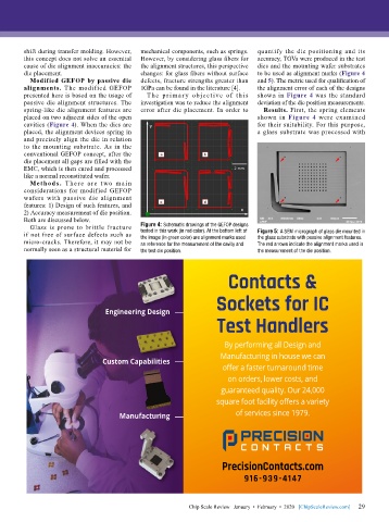
        presented here is based on the usage of   T he pr i ma r y obje ct ive of t h is   shown in Figure 4 was the standard
        passive die alignment structures. The   investigation was to reduce the alignment   deviation of the die position measurements.
        spring-like die alignment features are   error after die placement. In order to   Results. First, the spring elements
        placed on two adjacent sides of the open                              shown in  Figure 4 were examined
        cavities (Figure 4). When the dies are                                for their suitability. For this purpose,
        placed, the alignment devices spring in                               a glass substrate was processed with
        and precisely align the die in relation
        to the mounting substrate. As in the
        conventional GEFOP concept, after the
        die placement all gaps are filled with the
        EMC, which is then cured and processed
        like a normal reconstituted wafer.
          Methods. T here a re t wo mai n
        considerations for modified GEFOP
        wafers with passive die alignment
        features: 1) Design of such features, and
        2) Accuracy measurement of die position.
        Both are discussed below.
          Glass is prone to brittle fracture   Figure 4: Schematic drawings of the GEFOP designs
        if not free of surface defects such as   tested in this work (in red color). At the bottom left of   Figure 5: A SEM micrograph of glass die mounted in
                                                                              the glass substrate with passive alignment features.
                                           the image (in green color) are alignment marks used
        micro-cracks. Therefore, it may not be   as reference for the measurement of the cavity and   The red arrows indicate the alignment marks used in
        normally seen as a structural material for   the test die position.   the measurement of the die position.

                                                                      Contacts &


                                                                  Sockets for IC

                                 Engineering Design
                                                                  Test Handlers


                                                                     By performing all Design and
                                                                   Manufacturing in house we can
                                Custom Capabilities
                                                                    offer a faster turnaround time
                                                                      on orders, lower costs, and
                                                                   guaranteed quality. Our 24,000
                                                                  square foot facility offers a variety

                                     Manufacturing                      of services since 1979.


                                                                    PrecisionContacts.com

                                                                          916-939-4147


           Precision Contact Ad_7.6875 x 4.375_DEC-2109_Chip Scale.indd   1                         10/28/19   1:08 PM
                                                                                                             29
                                                          Chip Scale Review   January  •  February  •  2020   [ChipScaleReview.com]  29

