Page 30 - ChipScale_Jan-Feb_2020-digital
P. 30
Using laser-induced deep etching to enable


        microfeatures in glass


        By Roman Ostholt, Norbert Ambrosius, Jean-Pol Delrue, Rafael Santos, Daniel Dunker, Stephan Schmidt  [LPKF Laser & Electronics AG]


        This article was edited from papers respectively presented at the IMAPS Conferences in Pisa, Italy in Sept. 2019 and in
        Boston, USA in Nov. 2019.
        G          lass is  arguably  one  of


                   t h e m o s t  i n t e r e s t i n g
                   materials for heterogeneous
        integration. Whether it is for its radio
        f requency (R F) proper ties, high
        surface quality, hermeticity, tunable
        coefficient of thermal expansion (CTE)
        or low cost, there are several reasons
        to favor glass for advanced packaging
        applications. Unfortunately, and up to
        now, processibility of glass has not been
        among those reasons. This is because
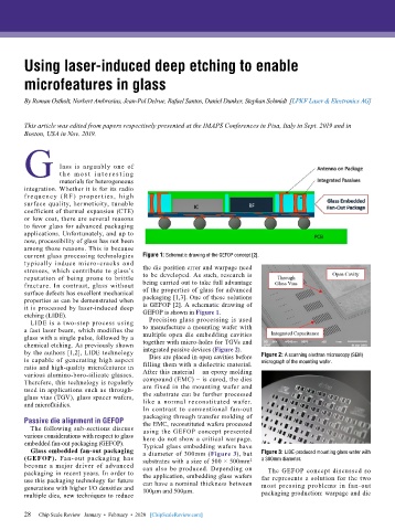
        current glass processing technologies   Figure 1: Schematic drawing of the GEFOP concept [2].
        typically induce micro-cracks and
        stresses, which contribute to glass’s   the die position error and warpage need
        reputation of being prone to brittle   to be developed. As such, research is
        fracture. In contrast, glass without   being carried out to take full advantage
        surface defects has excellent mechanical   of the properties of glass for advanced
        properties as can be demonstrated when   packaging [1,3]. One of these solutions
        it is processed by laser-induced deep   is GEFOP [2]. A schematic drawing of
        etching (LIDE).                    GEFOP is shown in Figure 1.
          LIDE is  a two-step  process  using   Precision glass processing is used
        a fast laser beam, which modifies the   to manufacture a mounting wafer with
        glass with a single pulse, followed by a   multiple open die embedding cavities
        chemical etching. As previously shown   together with micro-holes for TGVs and
        by the authors [1,2], LIDE technology   integrated passive devices (Figure 2).  Figure 2: A scanning electron microscopy (SEM)
        is capable of generating high aspect   Dies are placed in open cavities before   micrograph of the mounting wafer.
        ratio and high-quality microfeatures in   filling them with a dielectric material.
        various alumino-boro-silicate glasses.   After this material – an epoxy molding
        Therefore, this technology is regularly   compound (EMC) – is cured, the dies
        used in applications such as through-  are fixed in the mounting wafer and
        glass vias (TGV), glass spacer wafers,   the substrate can be further processed
        and microfluidics.                 like a normal reconstituted wafer.
                                           In contrast to conventional fan-out
                                           packaging through transfer molding of
        Passive die alignment in GEFOP     the EMC, reconstituted wafers processed
          The following sub-sections discuss   using the GEFOP concept presented
        various considerations with respect to glass   here do not show a critical warpage.
        embedded fan-out packaging (GEFOP).  Typical glass embedding wafers have
          Glass embedded fan-out packaging   a diameter of 300mm (Figure 3), but   Figure 3: LIDE-produced mounting glass wafer with
        (GEFOP).  Fan-out  packaging has   substrates with a size of 500 × 500mm²   a 300mm diameter.
        become a major driver of advanced   can also be produced. Depending on
        packaging in recent years. In order to   the application, embedding glass wafers   The  GEFOP  concept  discussed  so
        use this packaging technology for future   can have a nominal thickness between    far represents a solution for the two
        generations with higher I/O densities and   100µm and 500µm.          most  pressing problems in  fan-out
        multiple dies, new techniques to reduce                               packaging production: warpage and die

        28
        28   Chip Scale Review   January  •  February  •  2020   [ChipScaleReview.com]

