Page 26 - ChipScale_Jan-Feb_2020-digital
P. 26
at the slope, one can expect this to
        continue close to linearly, indicating that
        increasing the number of pixels by using
        a higher resolution camera setup enables
        one to reach the optical lateral resolution
        limitation of the system (4.875µm) [5].
                                           Table 2: Specifications for the 2 mirrors reported in this paper. All mirrors were 50.8mm in diameter with
                                           aluminum coating.
        Z-height resolution: amplitude
          A key aspect in determining the   over the sample using a lens that exhibits   analyzer. Any light coming from out-of-
        m i n i mu m a mplit ude t hat ca n be   a large longitudinal chromatic aberration   focus reflections will be rejected by the
        measured by a system is the noise   [9]. Because the chromatic aberration   pinhole aperture. Finally, by detecting the
        level. The noise level for AFM is about   causes different wavelengths to focus at   peak wavelength, the sample position can
        0.1nm and the noise level for an optical   different heights, there will be a specific   be found.
        profiler  is  on  the  order  of  0.4nm.   wavelength (λ 0 ), for which the focus lies   The technique described above has
        However, both techniques struggle   on the surface sample. The reflected light   been used in metrology because of its
        with speed and a very small field of   from the sample passes back through   capacity of measuring a large variety of
        view [8].                          the lens and is derived using a spectrum   surfaces. Its main limitation comes from
          A noise simulation was done where
        two circular images were generated
        and noise levels ranged from 20dB to
        infinity (meaning  infinite exposure
        time). The two noisy images were
        then put into the WFPI measurement
        algorithm and analyzed as if the two
        images had been acquired using the
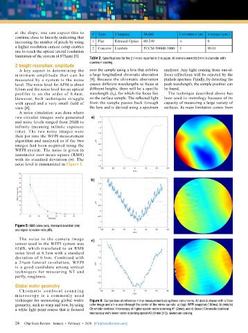
        WFPI system. The noise is given in
        nanometer root-mean-square (RMS)
        with  its  standard  deviation  (σ).  The
        noise level is summarized in Figure 5.


        Figure 5: RMS noise (nm), standard deviation (nm)
        and signal-to-noise-ratio (dB).
          The noise in the camera image
        sensor used in the WFPI system was
        62dB,  which  translated  to  an  RMS
        noise level at 0.3nm with a standard
        deviation  of  0.1nm.  Combined  with
        a 24µm lateral resolution, W FPI
        is a good candidate among optical
        techniques  for  measuring  NT  and
        partly, roughness.

        Global wafer geometry
          C h r o m a t ic c o n fo c a l s c a n n i ng
        m icroscopy is a com mon ly used
        technique for measuring global wafer   Figure 6: Comparison of reference mirror measurement using three instruments. All data is shown with a false
        geometry, such as warp and bow, by using   color image and a line scan through the center of the mirror sample. a) (top): WFPI snapshot (100ms); b) (middle)
        a white light point source that is focused   Chromatic confocal microscopy at higher speed raster scanning #1 (2min); and c) (lower) Chromatic confocal
                                           microscopy with lower raster scanning speed #2 (11min [11]). aluminum coating.

        24
        24   Chip Scale Review   January  •  February  •  2020   [ChipScaleReview.com]

