Page 23 - ChipScale_Jan-Feb_2020-digital
P. 23
Wavefront phase imaging for global and local


        wafer geometry


        By Juan M. Trujillo-Sevilla, Jose M. Ramos-Rodríguez, Jan Gaudestad  [Wooptix]
        W            avefront phase imaging   Introduction                    on a surface keeping its angle with respect


                     ( W F P I ) i s a  n e w
                                             T h e ge o m e t r y of u n p a t t e r n e d
                     technique  to  measure   silicon wafers used as substrates for IC   to the surface normal. The reflected beam
                                                                              will carry the wavefront phase, where the
        wafer geometry on a full wafer in a   manufacturing is critical for process   value is proportional to the surface height
        single image snapshot providing depth   control and ultimately, for device yield.   map. In our case, we are using a collimated
        information for every pixel. The number of   Wafer geometry has many characteristics   red (λ = 650nm) light beam that reflects
        topography data points for the entire wafer   that have been classified based on spatial   onto the surface—the reflection angle of
        will be proportional to the number of pixels   wavelength (λs) and amplitude (Z height   each ray is exactly two times the angle of
        in the image sensor, allowing for millions   resolution) (Figure 1) [2]. Nanotopography   the surface normal [4].
        of data points to be acquired in less than a   (NT) is defined as height variations with   There exists a value that defines the
        second. Sub-nanometer depth resolution is   amplitudes in the tens of nanometers at the   surface height range, which can be
        achieved by using two cameras with optics   wafer surface and within λs in the range of   measured for a certain configuration;
        that image the entire wafer, with the exact                           this is the limiting surface angle
        same field of view, at different conjugation                          (α lim =atan p⁄d ), which is given by the
        planes. Monochromatic incoherent light is
        illuminating the wafer and lateral resolution
        is determined by the lenses used for a
        specific field of view and the number of
        pixels offered by the image sensor.
          As WFPI is an obvious candidate for
        incoming wafers at the front end of line
        (FEOL, i.e., the fab process up to when active
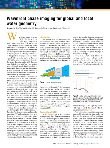
        devices (transistors) are made on the silicon   Figure 1: Definition of wafer geometry.
        wafer but before metal layers are deposited)
        on account of its high speed and high lateral   200µm–20mm. Beyond NT lies roughness,
        resolution. However, it may be an even   with amplitude in the single-digit
        more important tool for the far back end of   nanometer to sub-nanometer range and
        line (i.e., FBEOL starts when metal layers   λs in the range of tens of nanometers to
        have been added to the silicon wafer and   microns. Shape and flatness have typically   Figure 2: Limiting surface angle defines the height
        associated interconnect structures forming   been measured optically using confocal   range for a given configuration where p is the side length
        the connection between on-chip and off-chip   microscopy or laser interferometry. Such   of the measurement planes, d is the distance between
        wiring) where the silicon wafers are thinned,   systems (one or the other), however,   measurement planes, and l is the working distance.
        polished and then stacked as 3D integrated   have not been able to measure NT and
        circuits (ICs) [1]. During the thinning and   roughness on account of their poor spatial   maximum angle that a light ray can be
        polishing steps, it is critical to measure the   resolution [2,3].    reflected and still be recorded by the
        nanotopography (NT) and roughness of                                  imaging sensors (Figure 2).
        the wafer. As there are many candidates for   Description of WFPI       This estimation gives the maximum
        measuring NT and roughness, none have   The working principle of WFPI is based   measurable absolute surface angle, but
        the speed to measure an entire wafer within   on registering the intensity distribution   does not give a measure of the maximum
        the time frame required in a semiconductor   at two different optical measurement   height range for a certain configuration.
        manufacturing line allowing the fab engineer   planes. The intensity distribution is   The maximum range is important because
        to only measure small sample areas in the   recorded by a conventional imaging sensor.   it defines the maximum warpage of a
        range of about a square millimeter providing   The wavefront phase is defined as the   sample to be measured. In this case, it
        single-digit micron resolution. WFPI, on   surface perpendicular to the direction of   has been found that a surface angle that
        the other hand, can image the entire wafer,   propagation of the light rays. The sensor   causes 1% of the maximum displacement
        thereby providing millions of data points with   assumes geometrical propagation of   is within the measurable range. Then,
        single-digit micron lateral resolution and sub-  light, and in this regime the light can be   following a geometrical approximation, the
                                                                                       2
        nanometer height resolution (amplitude) with   considered as a collection of light rays that   range R=p ⁄(100∙d). The height resolution
        a single snapshot in less than a second.   bends according to Snell’s law and reflects   is defined by the minimum measurable


                                                                                                             21
                                                          Chip Scale Review   January  •  February  •  2020   [ChipScaleReview.com]  21

