Page 19 - ChipScale_Jan-Feb_2020-digital
P. 19
placement measurements and pattern                                    It uses pattern recognition alignment,
        overlay registration requirements are                                 allowing the user to train the system
        continuing to tighten. As a result, the                               to recognize and align on any unique
        position of the die must be measured                                  pattern within the field of view. The
        before each exposure in the lithography                               alignment system can measure the X,
        system to ensure accurate registration with                           Y position of die patterns across the
        the underlying layer. Displacement errors                             panel, a process often referred to as
        can be measured in the lithography tool,                              “mapping.” The AOI system (Firefly
        but these measurements are slow, typically                            System, Onto Innovation) uses a similar
        taking as much time as the exposure                                   pattern recognition alignment method
        itself. Transferring the measurement                                  to assess die placement error. Using
        operation to a parallel, independent                                  the  stepper  and  AOI  alignment  site
        metrology system and feeding corrections                              measurements from the test vehicle
        to the stepper, however, can double                                   panel, a mathematical algorithm was
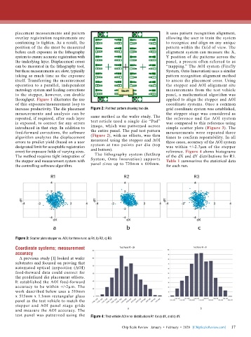
        throughput. Figure 1 illustrates the use                              applied to align the stepper and AOI
        of this exposure/measurement loop to                                  coordinate systems. Once a common
        increase productivity. The die placement   Figure 2: Pad test pattern showing two die.  grid coordinate system was established,
        measurements and analysis can be                                      the stepper stage was considered as
        repeated, if required, after each layer   same method as the wafer study. The   the  reference  and  the  AOI  system
        is exposed, to correct for any errors   test reticle used a single die “Pad”   was compared to this reference using
        introduced in that step. In addition to   image,  which was patterned across   simple scatter plots (Figure 3). The
        feed-forward corrections, the software   the entire panel. The pad test pattern   measurements were repeated three
        algorithm analyzes the displacement   (Figure 2), with no offsets, was then   times to confirm repeatability. In all
        errors to predict yield (based on a user   measured using the stepper and AOI   three cases, accuracy of the AOI system
        designated limit for acceptable registration   system at two points per die (top   was within +/-2.3µm of the stepper
        error) for exposure fields of varying sizes.   and bottom).           reference. Figure 4 shows histograms
        The method requires tight integration of   The lithography system (JetStep   of the dX and dY distributions for R1.
        the stepper and measurement system with   System,  Onto  Innovation)  supports   Table 1 summarizes the statistical data
        the controlling software algorithm.  panel sizes up to 720mm x 600mm.   for each run.


        Figure 3: Scatter plots stepper vs. AOI, for three runs: a) R1, b) R2, c) R3.
        Coordinate systems; measurement
        accuracy
          A previous study [1] looked at wafer
        substrates and focused on proving that
        automated  optical  inspection  (AOI)
        feed-forward data could correct for
        the predefined die placement offsets.
        It  established  the  AOI  feed-forward
        accuracy to be within +/-2µm. The
        work described below uses a 510mm
        x 515mm x 1.1mm rectangular glass
        panel as the test vehicle to match the
        stepper  and  AOI  panel  stage  grids
        and measure the AOI accuracy. The
        test panel was patterned using the   Figure 4: Test vehicle AOI error distributions R1 for a) dX, and b) dY.

                                                                                                             17
                                                          Chip Scale Review   January  •  February  •  2020   [ChipScaleReview.com]  17

