Page 16 - ChipScale_Jan-Feb_2020-digital
P. 16
Overcoming FOPLP die placement error


        By Keith Best  [Onto Innovation]
        I     t is well understood that advanced   Although FOPLP processing has many   tool to capture die placement error data


              packaging applications require high
                                                                              forward. The “feed-forward” solution
              performance, low cost, increased   advantages, it also faces significant   from a panel and feeds that information
                                           challenges. One critical challenge is die
        functionality and improved reliability   placement error, which occurs when die   optimizes the stepper, site-by-site, for X,
        that 2.5D and 3D packaging solutions   are positioned during the reconstitution   Y and rotation offsets, during exposure.
        provide. Fan-out panel-level packaging   and molding process. These placement   Visualization of  the  metrology  data
        (FOPLP) is one of the technologies that   errors are amplified with the larger panel   allows the user to characterize upstream
        has the potential to meet these packaging   format when compared to reconstituted   and downstream processes. Moreover,
        requirements. Similar to fan-out wafer-  wafers, and errors of 50μm or more   analytical capabilities predict yield as a
        level  packaging  (FOWLP),  FOPLP   are not unusual. In order to guarantee   function of exposure field size, thereby
        processes reconstitute die on a substrate,   acceptable yield, these errors must be   allowing the user to balance throughput
        in this case a rectangular platform that can   corrected during the lithography process   against yield in real time. This solution
        be significantly larger than the standard   using site-by-site corrections. Conducting   can significantly  increase  stepper
        300mm diameter wafer form. In the   metrology and site-by-site exposures   throughput, reduce cost and increase
        reconstitution process, die are displaced   on the lithography system is very time   productivity while ensuring high yield.
        from their nominal grid locations during   consuming. Substrate alignment and error
        the epoxy molding compound process   correction may be calculated using global   Die placement challenges
        and sometimes during subsequent    alignment, but this correction does not   Generating reconstit uted panel
        processing steps. This fan-out technology   accommodate nonlinear die placement   substrates creates translational and
        delivers more space for redistributed I/O   errors. It has become clear that only   rotational die placement errors. The
        connections, providing increased flexibility   site-by-site corrections can deliver the   “pick and place” process itself introduces
        for homogeneous and heterogeneous   overlay required to maintain good yield.   initial errors that are exacerbated during
        integration. Importantly, the larger panel   Executing site-by-site alignments in the   the mold process, and by instability of
        format can support more packages per   stepper reduces throughput and increases   the mold compound throughout repeated
        substrate than the 300mm wafer form, and   cost enough to make that approach to   processing cycles. With redistribution
        the final package size can be increased by   FOPLP processes impractical. A new   layer (RDL) features currently achieving
        adding space between the die.      approach uses an external metrology   dimensions as small as 2µm, die


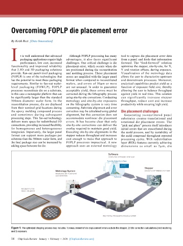
        Figure 1: The optimized stepping process loop includes: 1) measurement of die displacement errors outside the stepper; 2) Site correction calculations/yield modeling;
        and 3) exposure.

        14
        14   Chip Scale Review   January  •  February  •  2020   [ChipScaleReview.com]

