Page 11 - ChipScale_Jan-Feb_2020-digital
P. 11
difference used for cycling also has a big
        impact on TCoB. A ball’s size, as well as
        the composition of the balls are of great
        importance for increasing the TCoB
        robustness. By adjusting the package
        thickness, only a minor impact is seen.
        On the other hand, choosing the wrong
        RF board-sheet or -stack, may have one
        of the biggest impacts on reducing the
        TCoB reliability. The type of RF laminate
        used with the hybrid PCB is one of the
        major factors determining the solder
        joint lifetime [3,4]. For setting up the
        application system, attention must be
        paid to the TCoB differences of a free
        test board compared to a PCB within a
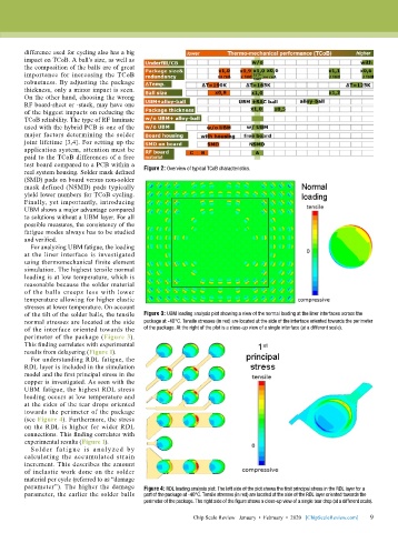
        real system housing. Solder mask defined   Figure 2: Overview of typical TCoB characteristics.
        (SMD) pads on board versus non-solder
        mask defined (NSMD) pads typically
        yield lower numbers for TCoB cycling.
        Finally, yet importantly, introducing
        UBM shows a major advantage compared
        to solutions without a UBM layer. For all
        possible measures, the consistency of the
        fatigue modes always has to be studied
        and verified.
          For analyzing UBM fatigue, the loading
        at the liner interface is investigated
        using thermomechanical finite element
        simulation. The highest tensile normal
        loading is at low temperature, which is
        reasonable because the solder material
        of the balls creeps less with lower
        temperature allowing for higher elastic
        stresses at lower temperature. On account
        of the tilt of the solder balls, the tensile   Figure 3: UBM loading analysis plot showing a view of the normal loading at the liner interfaces across the
        normal stresses are located at the side   package at -40°C. Tensile stresses (in red) are located at the side of the interface oriented towards the perimeter
        of the interface oriented towards the   of the package. At the right of the plot is a close-up view of a single interface (at a different scale).
        perimeter of the package (Figure 3).
        This finding correlates with experimental
        results from delayering (Figure 1).
          For understanding RDL fatigue, the
        RDL layer is included in the simulation
        model and the first principal stress in the
        copper is investigated. As seen with the
        UBM fatigue, the highest RDL stress
        loading occurs at low temperature and
        at the sides of the tear drops oriented
        towards the perimeter of the package
        (see Figure 4). Furthermore, the stress
        on the RDL is higher for wider RDL
        connections. This finding correlates with
        experimental results (Figure 1).
          Solde r fat ig ue is a n a ly z e d by
        calculating the accumulated strain
        increment. This describes the amount
        of inelastic work done on the solder
        material per cycle (referred to as “damage
        parameter”). The higher the damage   Figure 4: RDL loading analysis plot. The left side of the plot shows the first principal stress in the RDL layer for a
        parameter, the earlier the solder balls   part of the package at -40°C. Tensile stresses (in red) are located at the side of the RDL layer oriented towards the
                                           perimeter of the package. The right side of the figure shows a close-up view of a single tear drop (at a different scale).

                                                          Chip Scale Review   January  •  February  •  2020   [ChipScaleReview.com]  9 9

