Page 12 - ChipScale_Jan-Feb_2020-digital
P. 12
Figure 5: A heat map showing the distribution of the
        damage parameter across the package with respect
        to solder loading. Red indicates high loading and
        green indicates low loading.
        will fail, and vice versa. The heat map
        in Figure 5 shows the distribution of the
        damage parameter across the package:

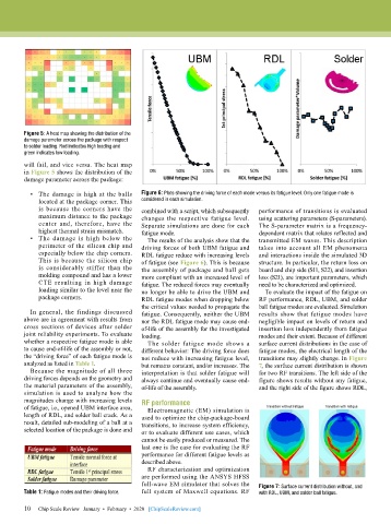
          •  The damage is high at the balls   Figure 6: Plots showing the driving force of each mode versus its fatigue level. Only one fatigue mode is
             located at the package corner. This   considered in each simulation.
             is because the corners have the   combined with a script, which subsequently   performance of transitions is evaluated
             maximum distance to the package   changes the respective fatigue level.   using scattering parameters (S-parameters).
             center  and,  therefore,  have  the   Separate simulations are done for each   The S-parameter matrix is a frequency-
             highest thermal strain mismatch.  fatigue mode.                  dependent matrix that relates reflected and
          •  The damage is high below the    The results of the analysis show that the   transmitted EM waves. This description
             perimeter of the silicon chip and   driving forces of both UBM fatigue and   takes into account all EM phenomena
             especially below the chip corners.   RDL fatigue reduce with increasing levels   and interactions inside the simulated 3D
             This is because the silicon chip   of fatigue (see Figure 6). This is because   structure. In particular, the return loss on
             is considerably stiffer than the   the assembly of package and ball gets   board and chip side (S11, S22), and insertion
             molding compound and has a lower   more compliant with an increased level of   loss (S21), are important parameters, which
             CTE resulting in high damage   fatigue. The reduced forces may eventually   need to be characterized and optimized.
             loading similar to the level near the   no longer be able to drive the UBM and   To evaluate the impact of the fatigue on
             package corners.              RDL fatigue modes when dropping below   RF performance, RDL, UBM, and solder
                                           the critical values needed to propagate the   ball fatigue modes are evaluated. Simulation
          In general, the findings discussed   fatigue. Consequently, neither the UBM   results show that fatigue modes have
        above are in agreement with results from   nor the RDL fatigue mode may cause end-  negligible impact on levels of return and
        cross sections of devices after solder   of-life of the assembly for the investigated   insertion loss independently from fatigue
        joint reliability experiments. To evaluate   loading.                 modes and their extent. Because of different
        whether a respective fatigue mode is able   The solder fatigue mode shows a   surface current distributions in the case of
        to cause end-of-life of the assembly or not,   different behavior: The driving force does   fatigue modes, the electrical length of the
        the “driving force” of each fatigue mode is   not reduce with increasing fatigue level,   transitions may slightly change. In Figure
        analyzed as listed in Table 1.     but remains constant, and/or increases. The   7, the surface current distribution is shown
          Because the magnitude of all three   interpretation is that solder fatigue will   for two RF transitions. The left side of the
        driving forces depends on the geometry and   always continue and eventually cause end-  figure shows results without any fatigue,
        the material parameters of the assembly,   of-life of the assembly.   and the right side of the figure shows RDL,
        simulation is used to analyze how the
        magnitudes change with increasing levels   RF performance
        of fatigue, i.e., opened UBM interface area,   Electromagnetic (EM) simulation is
        length of RDL, and solder ball crack. As a   used to optimize the chip-package-board
        result, detailed sub-modeling of a ball at a   transitions, to increase system efficiency,
        selected location of the package is done and   or to evaluate different use cases, which
                                           cannot be easily produced or measured. The
                                           last one is the case for evaluating the RF
                                           performance for different fatigue levels as
                                           described above.
                                             RF characterization and optimization
                                           are performed using the ANSYS HFSS
                                           full-wave EM simulator that solves the   Figure 7: Surface current distribution without, and
        Table 1: Fatigue modes and their driving force.  full system of Maxwell equations. RF   with RDL, UBM, and solder ball fatigue.

        10   Chip Scale Review   January  •  February  •  2020   [ChipScaleReview.com]
        10

