Page 17 - ChipScale_Jan-Feb_2020-digital
P. 17
New Advanced Bonding Technologies


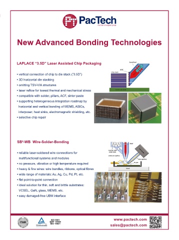
            LAPLACE “3.5D” Laser Assisted Chip Packaging


            • vertical connection of chip to die stack (”3.5D”)

            • 3D horizontal die stacking
            • omitting TSV-VIA structures
            • laser reflow for lowest thermal and mechanical stress
            • compatible with solder, pillars, ACF, sinter paste
            • supporting heterogeneous integration roadmap by

              horizontal and vertical bonding of MEMS, ASICs,
              interposer, heat sinks, electromagnetic shielding, etc.
            • selective chip repair


            SB²-WB  Wire-Solder-Bonding


            • reliable laser-soldered wire connections for

              multifunctional systems and modules
            • no pressure, vibration or high temperature required
            • heavy & fine wires: wire bundles, ribbons, optical fibres
            • wide range of materials: Au, Ag, Cu, Pd, Pt, etc.
            • flat point-to-point connection

            • ideal solution for thin, soft and brittle substrates:
              VCSEL, GaN, glass, MEMS, etc.
            • easy damaged-free UBM interface


                                  ISO 9001                                 www.pactech.com
                                  IATF 16949
                                  ISO 14001                              sales@pactech.com

