Page 27 - ChipScale_Jan-Feb_2020-digital
P. 27
The data demonstrates a strong correlation
                                                                              between WFPI and chromatic confocal
                                                                              microscopy. In the current WFPI system, the
                                                                              data acquisition is fast (less than a second),
                                                                              however, the data analysis can take up to 2s.
                                                                              Most of the time used for data analysis is
                                                                              spent acquiring the amplitude of the light.

                                                                              Local wafer geometry
                                                                                To  measure  local  variations  (NT
                                                                              and roughness), a 2-inch blank silicon
                                                                              wafer with specifications according
                                                                              to SEMI standards [13] was used for
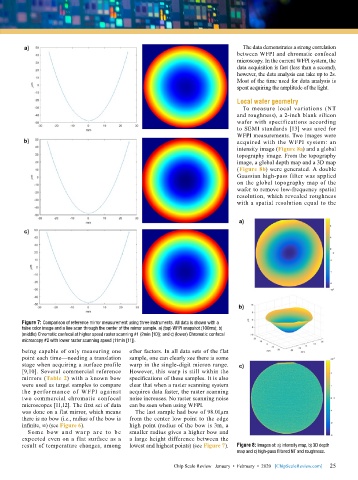
                                                                              WFPI measurements. Two images were
                                                                              acquired with the WFPI system: an
                                                                              intensity image (Figure 8a) and a global
                                                                              topography image. From the topography
                                                                              image, a global depth map and a 3D map
                                                                              (Figure 8b) were generated. A double
                                                                              Gaussian high-pass filter was applied
                                                                              on the global topography map of the
                                                                              wafer to remove low-frequency spatial
                                                                              resolution, which revealed roughness
                                                                              with a spatial resolution equal to the


        Figure 7: Comparison of reference mirror measurement using three instruments. All data is shown with a
        false color image and a line scan through the center of the mirror sample. a) (top) WFPI snapshot (100ms); b)
        (middle) Chromatic confocal at higher speed raster scanning #1 (2min [10]); and c) (lower) Chromatic confocal
        microscopy #2 with lower raster scanning speed (11min [11]).
        being capable of only measuring one   other factors. In all data sets of the flat
        point each time—needing a translation   sample, one can clearly see there is some
        stage when acquiring a surface profile   warp in the single-digit micron range.
        [9,10]. Several commercial reference   However, this warp is still within the
        mirrors (Table 2) with a known bow   specifications of these samples. It is also
        were used as target samples to compare   clear that when a raster scanning system
        the performance of WFPI against    acquires data faster, the raster scanning
        two commercial chromatic confocal   noise increases. No raster scanning noise
        microscopes [11,12]. The first set of data   can be seen when using WFPI.
        was done on a flat mirror, which means   The last sample had bow of 98.01µm
        there is no bow (i.e., radius of the bow is   from the center low point to the edge
        infinite, ∞) (see Figure 6).       high point (radius of the bow is 3m, a
          Some bow a nd wa r p a re to be   smaller radius gives a higher bow and
        expected even on a flat surface as a   a large height difference between the
        result of temperature changes, among   lowest and highest points) (see Figure 7).  Figure 8: Images of: a) intensity map, b) 3D depth
                                                                              map and c) high-pass filtered NT and roughness.

                                                                                                             25
                                                          Chip Scale Review   January  •  February  •  2020   [ChipScaleReview.com]  25

