Page 35 - ChipScale_Jan-Feb_2020-digital
P. 35
Eliminating warpage for FOWLP during debonding


        By Debbie Claire Sanchez, Klemens Reitinger, Miguel Adolfo Resendiz Jimenez,
        Sophia Oldeide, Kang Zhao, Wenxuan Song, Ibrahim Khwaja  [ERS electronic GmbH]


        T        he increasing demand for   panel with RDL is then debonded from   Die bonding. The process starts with


                 smaller a nd more cost-
                 efficient packaging in the   the carrier. The process then moves   the picking of known good dies (KGD)
                                                                              from a sawn silicon wafer, which are
                                           to back-end processing. Solder balls
        portable electronic area has increased   are placed on top of the RDLs, which   then placed onto a temporary carrier
        the discussion about fan-out wafer-  serve as an electrical conduit between   laminated with a thermal or ultraviolet
        level packaging (FOWLP). Advantages   the dies and board.             (UV) sensitive tape.
        of FOWLP technology include: 1) Good   The chip-first process (Figure 1) is   Molding. The compression molding
        electrical performance; 2) Supporting   more widely used by companies like   process is commonly used for this
        increasing demands for I/O count; 3)   Infineon, ASE, and Deca Technologies,   structure. It starts with weighing the
        Enabling dual-die or multi-die package                                right amount of EMC and dispensing
        configuration; and 4) Providing a                                     it on top of the carrier. The machine
        supporting fine redistribution layer                                  then starts closing the cavity in a
        ( R DL)  t races  ≤10µm  li ne/space.                                 controlled speed.
        Alongside the mass production, two                                      D e b o nd i n g.  T h e d e b o n d i ng
        critical issues surfaced for FOWLP:                                   process is t he se pa r at ion of t he
        die shift and wafer warpage.                                          reconstituted wafer from the carrier,
          Die shift results from misplacement                                 via the application of heat, or laser
        of the die with regards to its designed                               exposure. The sensitive (thermal or
        posit ion. Wa r page is due to t he                                   UV) tape layer softens and loosens
        mismatch of the coefficient of thermal                                adhesion to aid separation of the wafer
        expansion  (CTE)  between  silicon                                    from  the  carrier.  Once  the  wafer  is
        and the epoxy molding compound                                        separated from the carrier material,
        (EMC).  EMC,  having  a  higher  CTE                                  any characteristic imbalance will be
        value, results in an imbalance, which                                 evident, leading to warpage. Warpage
        will cause the wafer or panel to                                      appears on account of mechanical
        warp. Applying the correct thermal                                    stress caused by the CTE mismatch of
        treatment process, however, results in                                the reconstituted wafer.
        a warpage profile <1mm, which allows                                    For a thermal debonding process,
        succeeding processes to run smoothly.                                 ther mal unifor mit y is cr itical to
        The idea is to treat the wafer with a                                 ensure no wafer excursion occurs.
        temperature higher or equal to its Tg                                 The thermal sensitive tape needs to
        until the mold compound softens, and                                  activate across the entire surface
        then transport it onto a cooler chuck.                                before mechanical separation of the
        As the wafer sits on the cool vacuum                                  carrier and the wafer. At this point,
        chuck, it conforms to its flatness. The                               the warpage becomes evident. In the
        transportation  from  the  debonding                                  chip-first structure, this process is
        station to the cooling chuck plays a                                  the launching pad for interconnect
        significant role, requiring several                                   build-up. If warpage is not reduced,
        critical items.                                                       w a r p a g e -i n d u c e d  d ef e c t s  w i l l
                                                                              increase as the wafer goes through
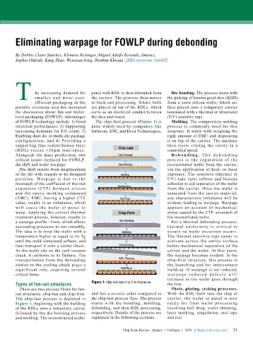
        Types of fan-out structures        Figure 1: Chip-last and chip-first structures.  the line.
          There are two process flows for fan-                                  Photo, plating, etching processes.
        out structures: chip-last and chip-first.   and has a reverse order compared to   With the RDL built into the chip or
        The chip-last process is depicted in   the chip-last process flow. The process   carrier, the wafer or panel is now
        Figure 1, beginning with the building   starts with die bonding, molding,   ready for f inal wafer processing
        of the RDLs onto a temporary carrier   debonding, and then RDL processing,   involving ball drop, wafer thinning,
        followed by the die bonding process   respectively. Details of the process are   laser marking, singulation, and tape
        and molding. The reconstructed wafer/  explained in the following sections.  and reel.

                                                                                                             33
                                                          Chip Scale Review   January  •  February  •  2020   [ChipScaleReview.com]  33

