Page 39 - ChipScale_Jan-Feb_2020-digital
P. 39
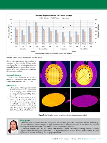
Figure 6: Graph of warpage improvement vs. parameter settings.
        allows minimum, to no introduction of
        warpage, as shown in the 200mm wafer
        experiment. Further investigation, however,
        is needed to see if contactless transport
        proves to be more efficient compared to a
        pick-and-place method.

        Acknowledgment
          This article is based on a paper
        presented at the International Wafer-Level
        Packaging Conference (IWLPC) 2019.

        References
         1.  J. Lau, et al., “Warpage and thermal
            characterization of fan-out wafer-
            level packaging,” 2017 IEEE Trans.
            on Comp., Packaging and Mfg. Tech.,
            pp.: 1-10.
         2.  S. Oldeide, R. Beckmann, L. Giai-
            Miniet,  K.  Reitinger,  “Thermal
            debonding and warpage adjust
            of FOWLP - a crucial step in the
            evolution of advanced packaging?”
            Inter. Wafer Level Packaging Conf.
            (IWLPC), San Jose, CA, 2018, pp. 1-6.


                                           Figure 7: Heat dissipation between contactless vs. the pick-and-place transport method.


                       Biographies
                         Debbie Claire Sanchez is Fan-Out Equipment Product Manager at ERS electronic GmbH, Germering,
                       Germany. She has a Master’s Degree in Physics from the Iligan Institute of Physics in the Philippines, and has
                       several years of experience in the fan-out field; email sanchez@ers-gmbh.de
                         Klemens Reitinger is the CEO and CTO at ERS electronic GmbH, Germering, Germany. He has a Master’s
                       Degree in Mechanical Engineering from the U. of Applied Science in Vienna, Austria, and more than 10 years
                       experience in thermal debonding and warpage adjustment.


                                                                                                             37
                                                          Chip Scale Review   January  •  February  •  2020   [ChipScaleReview.com]  37

