Page 43 - ChipScale_Jan-Feb_2020-digital
P. 43
3DInCites, Nov. 3, 2015; https://  flow,” Mentor, a Siemens Business,   level-packaging-with-mentor-
            www.3dincites.com/2015/11/why-do-  June, 2016; https://www.mentor.    graphics-ca735a12-d13c-46f2-aa99-
            we-need-assembly-design-kits-for-  com /pcb/resou rces/over view/     7fc413291825
            packages/                          i mplement i ng-fa n- out-wafer-
         3.  A. Heinig, “Why use an assembly
            design kit and assembly design flow?”
            Semiconductor Engineering, Feb. 8,
            2018; https://semiengineering.com/
            why-use-an-assembly-design-kit-and-
            assembly-design-flow/
         4.  R. Fuentes, A. Miller, J. Micksch,
            “Package assembly design kits bring
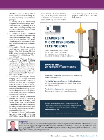
            value to semiconductor designs,” Chip   LEADERS IN
            Scale Review, Nov/Dec 2018; http://
            fbs.advantageinc.com/chipscale/nov-    MICRO DISPENSING
            dec_2018/files/assets/basic-html/page-
            41.html#                               TECHNOLOGY
         5.  T. Ramadan, “HDAP connectivity
            verification: what  you need to
            know,” Chip Scale Review, Mar/Apr      SMALL REPEATABLE VOLUMES
            2018; http://www.chipscalereview.      ARE A CHALLENGE, BUT NOT
            com/issue/1804/ChipScale_Mar_          IMPOSSIBLE IF YOU HAVE BEEN
            Apr_2018.pdf                           CREATING THEM AS LONG AS WE HAVE.
         6.  T. Ramadan, “Package designers
            need assembly-level LVS for HDAP
            verification,” Mentor, a Siemens
            Business, Dec. 2017; https://www.      TO DO IT WELL,
            mentor.com/products/ic_nanometer_      WE PROVIDE THREE THINGS:
            design/resources/overview/package-
            designers-need-assembly-level-lvs-for-
            hdap-verification-6faa5d86-f8ee-4a6b-
            91e8- e06ca213eb81/                    Dispensing Expertise in a variety of microelectronic
         7.  T. Ramadan, “Crossing the chasm:      packaging applications.
            bringing SoC and package verification
            together with 3DSTACK,” Mentor, a      Feasibility Testing & Process Verification based
            Siemens Business, Jan. 2017; https://  on years of product engineering, material flow testing
            www.mentor.com/products/ic_            and software control.
            nanometer_design/resources/overview/
            crossing-the-chasm-bringing-soc-       Product Development for patented valves,
            and-package-verification-together-     dispensing cartridges, needles, and accessories.
            with-calibre-3dstack-cee51550-0dca-
            4306-b33a-4131df0c6436/
         8.  T. Ramadan, “Adding system-level,
            post-layout electrical analysis to
            HDAP design and verification,” Tech
            Design Forum, Nov. 20, 2018; https://
            www.techdesignforums.com/practice/     Our Micro Dispensing product line is proven and trusted by
            technique/adding-system-level-post-    manufacturers in semiconductor, electronics assembly, medical
                                                   device and electro-mechanical assembly the world over.
            layout-electrical-analysis-to-hdap-
            design-and-verification/               www.dltechnology.com.
         9.  J. Ferguson, K. Felton, “Implementing
            fan-out wafer-level packaging          216 River Street, Haverhill, MA 01832  •  P: 978.374.6451  •  F: 978.372.4889  •  info@dltechnology.com
            (FOWLP) with the Mentor HDAP


                       Biography
                         Tarek Ramadan is a Technical Marketing Lead for Calibre Design Solutions at Mentor, a Siemens Business,
                       based in Cairo, Egypt. He supports Calibre physical verification solutions for 2.5D-IC, 3D-IC, and wafer-level
                       packaging applications. Tarek holds BS and MS degrees in Electrical Engineering from Ain Shams U., Cairo,
                       Egypt. Email: tarek_ramadan@mentor.com.


                                                                                                             41
                                                          Chip Scale Review   January  •  February  •  2020   [ChipScaleReview.com]  41

