Page 45 - ChipScale_Jan-Feb_2020-digital
P. 45
Creating Safe                             © 2017 Brewer Science, Inc.


                                                                  Environments

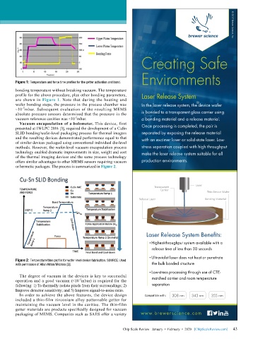
        Figure 1: Temperature and force time profiles for the getter activation and bond.
        bonding temperature without breaking vacuum. The temperature
        profile for the above procedure, plus other bonding parameters,   Laser Release System
        are shown in Figure 1. Note that during the heating and
        wafer bonding steps, the pressure in the process chamber was    In the laser release system, the device wafer
           -5
        ~10 mbar. Subsequent evaluation of the resulting MEMS
        absolute pressure sensors determined that the pressure in the   is bonded to a transparent glass carrier using
                                    -2
        vacuum reference cavities was <10 mbar.                   a bonding material and a release material.
          Vacuum encapsulation of a bolometer. This device, first
        presented at IWLPC 2016 [3], required the development of a CuSn   Once processing is completed, the pair is
        SLID bonding/wafer-level packaging process for thermal imagers   separated by exposing the release material
        and the resulting devices demonstrated performance equal to that   with an excimer laser or solid-state laser. Low-
        of similar devices packaged using conventional individual die-level
        methods. However, the wafer-level vacuum encapsulation process   stress separation coupled with high throughput
        technology enabled dramatic improvements in size, weight and cost   make the laser release system suitable for all
        of the thermal imaging devices and the same process technology
        offers similar advantages to other MEMS sensors requiring vacuum   production environments.
        or hermetic packages. The process is summarized in Figure 2.


                                                                                           Laser
                                                                        Transparent
                                                                           Carrier
                                                                                                 Thin Device Wafer
                                                                 Release Layer                  Bonding Material


                                                                     Laser Release System Benefits:
                                                                      •Highest-throughput system available with a
                                                                       release time of less than 30 seconds

                                                                      •Ultraviolet laser does not heat or penetrate
        Figure 2: Temperature/time profile for wafer-level device fabrication. SOURCE: Used
        with permission of Allan Hilton/Micross [3].                   the bulk bonded structure
                                                                      •Low-stress processing through use of CTE-
          The degree of vacuum in the devices is key to successful
                                      -2
        operation and a good vacuum (<10 mbar) is required for the     matched carrier and room temperature
        following: 1) To thermally isolate pixels from their surroundings; 2)   separation
        Improve detector sensitivity; and 3) Improve signal-to-noise ratio.
          In order to achieve the above features, the device design   Compatible with:  308 nm  343 nm  355 nm
        included a thin-film zirconium alloy patternable getter for
        maintaining the vacuum level in the cavities. The thin-film
        getter materials are products specifically designed for vacuum
        packaging of MEMS. Companies such as SAES offer a variety   www.brewerscience.com


                                                                                                             43
                                                          Chip Scale Review   January  •  February  •  2020   [ChipScaleReview.com]  43

