Page 44 - ChipScale_Jan-Feb_2020-digital
P. 44
Bonding processes for wafer-scale vacuum encapsulation


        By Tony Rogers, Anna Draisey, Roger Dyer  [Applied Microengineering Limited]
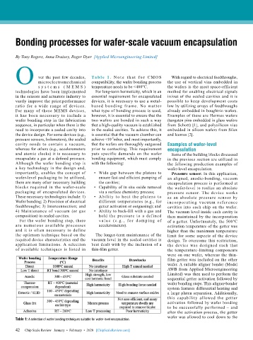
        O          ver the past few decades,   Tab l e  1 .  N o t e   t h a t   f o r  C M O S   With regard to electrical feedthroughs,


                   microelectromechanical
                                           temperature needs to be <400ºC.
                   s ys t e m s   ( M EM S )   compatibility, the wafer bonding process   the use of vertical vias embedded in
                                                                              the wafers is the most space-efficient
        technologies have been implemented   For long-term hermeticity, which is an   method for enabling electrical signals
        in the sensors and actuators industry to   essential requirement for encapsulated   in/out of the sealed cavities and it is
        vastly improve the price:performance   devices, it is necessary to use a metal-  possible to keep development costs
        ratio for a wide range of devices.   based  bonding  f rame.  No  mat ter   low by utilizing arrays of feedthroughs
        For  many  of  these  MEMS  devices,   what type of bonding process is used,   already embedded in bought-in wafers.
        it has been necessary to include a   however, it is essential to ensure that the   Examples of these are Hermes wafers
        wafer bonding step in the fabrication   two wafers are bonded in such a way   (tungsten pins embedded in glass wafers
        sequence, in particular when there is the   that a high-quality vacuum is established   from Schott) [1], and polysilicon vias
        need to incorporate a sealed cavity into   in the sealed cavities. To achieve this, it   embedded in silicon wafers from Silex
        the device design. For some devices (e.g.,   is essential that the vacuum chamber can   and Icemos [2].
                                                     -5
        pressure sensors, bolometers), the sealed   achieve <10 mbar, and most importantly,
        cavity needs to contain a vacuum,   that the wafers are thoroughly outgassed   Examples of wafer-level
        whereas for others (e.g., accelerometers   prior to contacting. This requirement   encapsulation
        and atomic clocks) it is necessary to   puts specific demands on the  wafer   Some of the building blocks discussed
        encapsulate a gas at a defined pressure.   bonding equipment, which must comply   in the previous section are utilized in
        Although the wafer bonding step is   with the following:              the following production examples of
        a key technology in the design and,                                   wafer-level encapsulation.
        importantly, enables the concept of   •  Wide gap between the platens to   Pressure sensor. In this application,
        wafer-level packaging to be utilized,   ensure fast and efficient pumping of   an aligned, anodic-bonding, vacuum
        there are many other necessary building   the cavities;               encapsulation process is performed at
        blocks required in the wafer-scale   •  Capability of in situ oxide removal   the wafer-level to realize an absolute
        packaging of encapsulated devices.     via a surface chemistry process;  pressure sensor. The device works
        These necessary technologies include: 1)   •  Ability  to  heat  the  platens to   as an absolute pressure sensor by
        Wafer bonding; 2) Provision of electrical   different temperatures (e.g., for   i ncor porat i ng vacuu m reference
        feedthroughs; 3) Interconnection; and   getter activation or outgassing); and   cavities into each chip on the wafer.
        4)  Maintenance  of  vacuum  (or  gas   •  Ability to back-fill with a gas and   The vacuum level inside each cavity is
        composition) in sealed cavities.       hold the pressure to a defined   then maintained by the incorporation
          For the wafer bonding step, there    v a l u e  (e . g ., f o r d a m p i n g of   of a getter. Unfortunately, the 500ºC
        are numerous available processes       accelerometers).               activation temperature of the getter was
        and it is often necessary to define                                   higher than the maximum temperature
        the optimum technique based on the   The longer-term maintenance of the   limit for some aspects of the device
        required device characteristics and the   vacuum level in the sealed cavities is   design. To overcome this restriction,
        application limitations. A selection   best dealt with by the inclusion of a   the device was designed such that
        of available techniques is listed in     thin-film getter.            the temperature-limiting components
                                                                              were on one wafer, whereas the thin-
                                                                              film getter was included on the other
                                                                              wafer. A suitable aligner bonder (Model
                                                                              AWB from Applied Microengineering
                                                                              Limited) was then used to perform the
                                                                              sequential getter activation followed by
                                                                              wafer bonding steps. This aligner-bonder
                                                                              system features differential heating and
                                                                              a large platen separation. Additionally,
                                                                              this capability allowed the getter
                                                                              activation followed by wafer bonding
                                                                              to be successfully performed – and
                                                                              after the activation process, the getter
                                                                              wafer was allowed to cool down to the
        Table 1: A selection of wafer bonding techniques suitable for wafer-level encapsulation.

        42
        42   Chip Scale Review   January  •  February  •  2020   [ChipScaleReview.com]

