Page 42 - ChipScale_Jan-Feb_2020-digital
P. 42
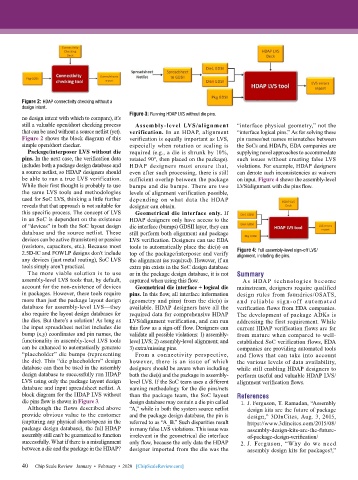
Figure 2: HDAP connectivity checking without a
        design intent.
                                           Figure 3: Running HDAP LVS without die pins.
        no design intent with which to compare), it’s
        still a valuable open/short checking process   Assembly-level LVS/alignment   “interface physical geometry,” not the
        that can be used without a source netlist (yet).   verification. In an HDAP, alignment   “interface logical pins.” As for solving these
        Figure 2 shows the block diagram of this   verification is equally important as LVS,   pin names/net names mismatches between
        simple open/short checker.         especially when rotation or scaling is   the SoCs and HDAPs, EDA companies are
          Package/interposer LVS without die   required (e.g., a die is shrunk by 10%,   supplying novel approaches to accommodate
        pins. In the next case, the verification data   rotated 90°, then placed on the package).   such issues without creating false LVS
        includes both a package design database and   HDAP designers must ensure that,   violations. For example, HDAP designers
        a source netlist, so HDAP designers should   even after such processing, there is still   can denote such inconsistencies as waivers
        be able to run a true LVS verification.   sufficient overlap between the package   on input. Figure 4 shows the assembly-level
        While their first thought is probably to use   bumps and die bumps. There are two   LVS/alignment with die pins flow.
        the same LVS tools and methodologies   levels of alignment verification possible,
        used for SoC LVS, thinking a little further   depending on what data the HDAP
        reveals that that approach is not suitable for   designer can obtain.
        this specific process. The concept of LVS   Geometrical die interface only. If
        in an SoC is dependent on the existence   HDAP designers only have access to the
        of “devices” in both the SoC layout design   die interface (bumps) GDSII layer, they can
        database and the source netlist. These   still perform both alignment and package
        devices can be active (transistors) or passive   LVS verification. Designers can use EDA
        (resistors, capacitors, etc.). Because most   tools to automatically place the die(s) on
        2.5D-IC and FOWLP designs don’t include   top of the package/interposer and verify   Figure 4: Full assembly-level sign-off LVS/
                                                                              alignment, including die pins.
        any devices (just metal routing), SoC LVS   the alignment (as required). However, if an
        tools simply aren’t practical.     extra pin exists in the SoC design database
          The more viable solution is to use   or in the package design database, it is not   Summary
        assembly-level LVS tools that, by default,   captured when using this flow.  As HDAP technologies become
        account for the non-existence of devices   Geometrical die interface + logical die   mainstream, designers require qualified
        in packages. However, these tools require   pins. In this flow, all interface information   design rules from foundries/OSATS,
        more than just the package layout design   (geometry and pins) from the die(s) is   a nd rel iable sig n- of f automat ed
        database for assembly-level LVS—they   available. HDAP designers have all the   verification flows from EDA companies.
        also require the layout design databases for   required data for comprehensive HDAP   The development of package ADKs is
        the dies. But there’s a solution! As long as   LVS/alignment verification, and can run   addressing the first requirement. While
        the input spreadsheet netlist includes die   this flow as a sign-off flow. Designers can   current HDAP verification flows are far
        bump (x,y) coordinates and pin names, the   validate all possible violations: 1) assembly-  from mature when compared to well-
        functionality in assembly-level LVS tools   level LVS; 2) assembly-level alignment; and   established SoC verification flows, EDA
        can be enhanced to automatically generate   3) extra/missing pins.    companies are providing automated tools
        “placeholder” die bumps (representing   From a connectivity perspective,   and flows that can take into account
        the die). This “die placeholders” design   however, there is an issue of which   the various levels of data availability,
        database can then be used in the assembly   designers should be aware when including   while still enabling HDAP designers to
        design database to successfully run HDAP   both the die(s) and the package in assembly-  perform useful and valuable HDAP LVS/
        LVS using only the package layout design   level LVS. If the SoC team uses a different   alignment verification flows.
        database and input spreadsheet netlist. A   naming methodology for the die pins/nets
        block diagram for the HDAP LVS without   than the package team, the SoC layout   References
        die pins flow is shown in Figure 3.  design database may contain a die pin called   1.  J. Ferguson, T. Ramadan, “Assembly
          Although the flows described above   “A,” while in both the system source netlist   design kits are the future of package
        provide obvious value to the customer   and the package design database, the pin is   design,” 3DInCites, Aug. 3, 2015,
        (capturing any physical shorts/opens in the   referred to as “A_B.” Such disparities result   https://www.3dincites.com/2015/08/
        package design database), the full HDAP   in many false LVS violations. This issue was   assembly-design-kits-are-the-future-
        assembly still can’t be guaranteed to function   irrelevant in the geometrical die interface   of-package-design-verification/
        successfully. What if there is a misalignment   only flow, because the only data the HDAP   2.  J. Ferguson, “Why do we need
        between a die and the package in the HDAP?  designer imported from the die was the   assembly design kits for packages?,”

        40   Chip Scale Review   January  •  February  •  2020   [ChipScaleReview.com]
        40

