January February 2024
Volume 28, Number 1
The megachip approach helps to rearchitect heterogeneous chip tiling for developing highly complex systems having desired circuit density and performance. Recent work on large-area superconducting integrated circuits to join multiple individual die is highlighted in this article, with particular attention paid to the processing of the high-density electrical interconnects formed between the individual die.
Cover image courtesy of iStock/NiPilot

March April 2024
Volume 28, Number 2
Semiconductors are the foundation for artificial intelligence (AI), quantum computing, Internet of Things (IoT), and advanced wireless communications, notably 5G. Due to Moore’s Law reaching its limit, and the system-on-chip (SoC) platform showing its shortcomings, advanced packaging has become a critical area for development to enable continuous performance improvement at reasonable cost. Glass-based advanced packaging and novel device architectures can play an important role.
.
Photo courtesy of Corning Incorporated

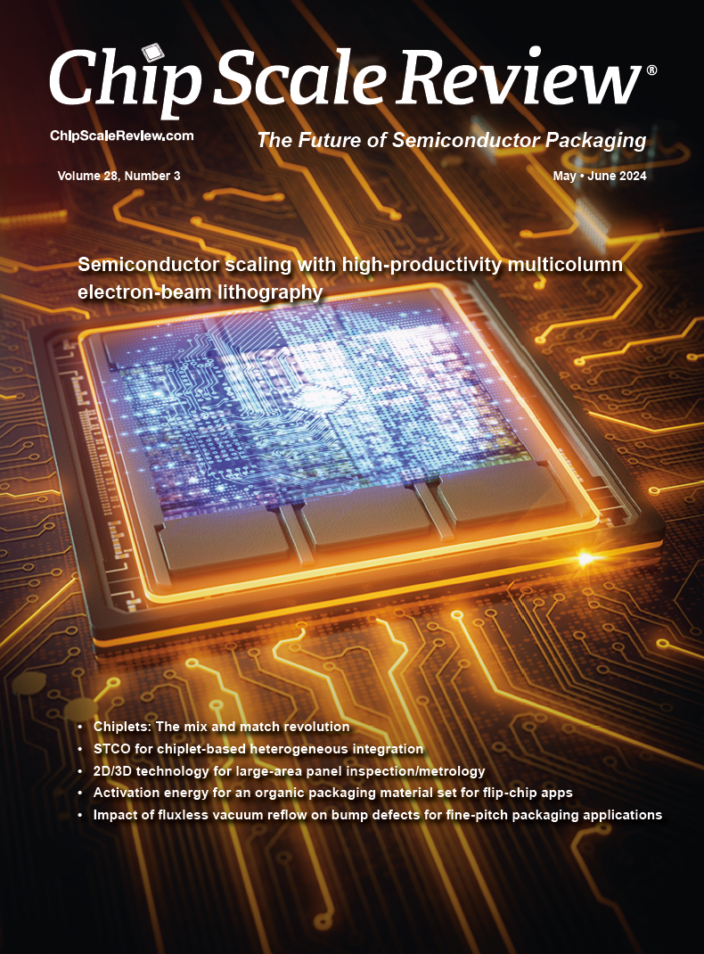
May June 2024
Volume 28, Number 3
Next-generation data centers supporting high-growth artificial intelligence (AI) applications require massive new scale in high-performance computing (HPC) and high-bandwidth memory (HBM), as well as higher energy efficiency. Multicolumn electron-beam lithography delivers high resolution, large field of view, huge depth of focus, and adaptable patterning capabilities that enable patterning of very high-density, low-power interconnects that deliver the speed and power required to fuel next- generation chip performance in high-growth AI-driven applications.
.
Cover image courtesy of Multibeam Corporation

July August 2024
Volume 28, Number 4
To continue scaling while increasing transistor density, the industry is turning to methods such as using the backside of the chip for wiring in addition to traditional front-side back-end-of-line wiring. The use of backside power delivery networks (BS-PDNs) can be done using several different schemes. However, as use of the wafer backside evolves, backside/frontside overlay tolerance is expected to grow tighter, resulting in challenges for patterning as discussed in the cover article.
.
Cover image courtesy of iStock/Kynny

September October 2024
Volume 28, Number 5
The demand for miniaturization, higher performance, and cost efficiency in semiconductor devices has fueled the evolution of redistribution layer (RDL) technology. Emerging from its roots in fan-out packaging, RDL has grown to address a range of applications, from lead-frame-free QFN to complex interposers for chiplets. As markets like AI, HPC, and ADAS continue to expand, RDL is playing a key role in shaping the future of advanced packaging.
.
Cover image courtesy of Deca Technologies Inc.

November December 2024
Volume 28, Number 6
3D ICs offer significant advantages in size, performance, power efficiency and cost. However, they come with design and verification challenges. To overcome these challenges, the author describes how multiphysics analysis early and throughout the design process will enable high-yield, reliable 3D IC designs with optimal electrical behavior.
.
Cover image courtesy iStock/blackdovfx


