Page 28 - ChipScale_Nov-Dec_2020-digital
P. 28
Similarly, the JC-70.2 subcommittee                                 the total conductivity from source and
        is determining guidelines for the testing                             drain needs to be maximized. Second,
        and reliability of SiC power devices.                                 thermal and electrical interfaces need to
        Both efforts should incentivize and                                   be eliminated or considerably reduced in
        simplify the adoption of these advanced                               length/thickness. Third, the conductive
        semiconductor technologies, especially                                material density of the package needs to
        if packaging advancements match the                                   be increased. Reimagining or reinventing
        semiconductor’s capabilities.                                         the chip-scale package (CSP) for power
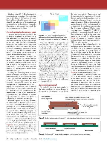
                                                                              applications, PowerCSP™ (PCSP)
        Current packaging technology gaps                                     technology accomplishes all three of
          Today’s discrete power packages are                                 these objectives, while at the same time
        limited to the electrical performance of   Figure 2: Low- to mid-range power applications   reducing the overall size of the device.
        clip, wire and solder interfaces. In general,   provide opportunities for innovative integrated power   Figure 3 shows key aspects of this
        discrete packaging follows the design   packaging that overlaps the discrete and PQFN spaces.  package design including heat spreader
        philosophy that greater size/volume   Previous attempts to bridge the gap   (HS) and other options.
        correlates to higher power handling   with embedded technologies have resulted   To maximize the total conductivity in
        capability. However, more efficient   in highly complex designs that were   traditional power packaging, the source
        transistor technology (such as GaN and   vulnerable to low yield issues, but they   and drain need to be connected to current
        SiC) provides the ability to handle more   did address specific application needs.   carrying materials at or near 100% of
        power in the same size package or to   While many can be considered technical   the available space in the die design.
        reduce the form factor significantly.  successes, especially to address the niche   Traditionally, this is done by increasing
          A PQFN can handle multiple die   markets they targeted, their adoption has   the number of wires, increasing the wire
        where power MOSFETs can be stacked   been limited. With a supply chain mostly   diameter or maximizing the size of the
        or side by side within the same package.   enabled through substrate manufacturers,   clip attached to the source or drain. In the
        To further reduce printed circuit board   the ownership of yield as well as cost   PowerCSP technology, designs allow the
        (PCB) space and improve electrical   responsibility hindered their adoption and   die to use all the available source and drain
        eff iciency, inductors and passive   ability to transition to a mainstream power   area by connecting the die directly through
        devices can be integrated within or on   packaging technology.        a Cu pad that serves both as the current-
        top of the package.                  Ultimately, the need to increase power   carrying and heat-dissipating element.
          An ongoing challenge that discrete   to package density by removing lossy   Figure 4 shows connectivity options.
        power packaging and PQFNs encounter   interfaces has created an opportunity   Each interface in a power device can
        is the difficulty to effectively integrate   window for a new integrated power   act as a thermal or electrical throttle
        a package size that handles the power   packaging concept for low- to mid-range   or an opportunity for failure in harsh
        required for the application with an   power applications.            environments. As a result, the fewer
        adequate interface to address the heat                                interfaces in the device and the system,
        dissipation. A large form factor (LFF)   A new design concept         the better, and the trend is to eliminate
        PQFN can have exposed pads for passive   To radically improve functionality in   them to provide a predictable electrical
        integration but is constrained in the    the integrated power space discussed   path. PCSP technology minimizes the
        I/O density and Cu thickness of the   above, three things must occur. First,   interfaces to a single connection from
        lead frame. A LFF PQFN achieves its
        capabilities with the tradeoffs of thermal
        capacity and the increased process
        complexity of many die attach steps.
          For the highest power requirements
        in  applications  handling hundreds
        and even thousands of watts, power is
        packaged in power modules and package
        dimensions shift from millimeters
        to centimeters. These packages are
        normally attached to large heat sinks
        with bolts and nuts, and electrical
        connections are made with large size
        wires or cables attached with screws.   Figure 3: The first implementation of PowerCSP™ technology shows its flexibility and many construction options.
        These high-power modules may even
        be water cooled at the system level. As
        Figure 2 shows, this leaves a gap in the
        low- to medium-power range that is not
        filled by either discrete devices or large
        power modules. This space is ripe for
        innovation and optimization.
                                           Figure 4: The PowerCSP™ design provides many connectivity options for chip-scale power.

        26
        26   Chip Scale Review   November  •  December  •  2020   [ChipScaleReview.com]

