Page 30 - ChipScale_Nov-Dec_2020-digital
P. 30
This reduces its integral thermal capacity
                                                                              and requires external heat sinking to achieve
                                                                              an acceptable thermal solution in some
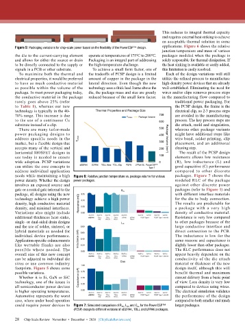
                                                                              applications. Figure 6 shows the relative
        Figure 5: Packaging variations for chip-scale power based on the flexibility of the PowerCSP™ design.
                                                                              junction temperature and mass of various
        the die to the current-carrying element   operate at temperatures of 175°C to 200°C.   packages modeled when the package is
        and allows for either the source or drain   Packaging is an integral part of addressing   solely responsible for thermal dissipation. If
        to be directly connected to the supply or   the high-temperature challenge.  the heat sinking is available or easily added,
        signals in a PCB or other substrate.  To achieve a small form factor, one of   this limitation is easily resolved.
          To maximize both the thermal and   the tradeoffs of PCSP design is a limited   Each of the design variations will still
        electrical properties, it would be preferred   amount of copper in the package in the   utilize the refined process to manufacture
        to have as much conductive material   lateral direction. Even though the new   high-density power devices that are already
        as possible within the volume of the   technology uses a thick lead frame above the   well-established. Eliminating the need for
        package. In most power packaging today,   die, the package mass and size are greatly   wires and/or clips removes process steps
        the conductive material in the package   reduced because of the small form factor.   in the manufacturing flow compared to
        rarely goes above 25% (refer                                                 traditional power packaging. For
        to Table 1), whereas our new                                                 the PCSP design, the frame is the
        technology is typically in the 40-                                           electrical clip, so 2-3 process steps
        70% range. This increase is due                                              are avoided in the manufacturing
        to the use of a continuous Cu                                                process. The key process steps are
        substrate instead of a clip.                                                 die attach, mold and singulation,
          There are many tailor-made                                                 whereas other package variants
        power packaging designs to                                                   might have additional steps like
        address specific needs in the                                                wire bond, solder printing, clip
        market, but a flexible design that                                           placement, and an additional
        accepts many of the vertical and                                             cleaning step.
        horizontal MOSFET designs in                                                  The result of the PCSP design
        use today is needed to ensure                                                elements allows low resistance
        wide adoption. PCSP variations                                               (R), low inductance (L) and
        can utilize the core concepts to                                             good capacitive (C) performance
        address individual application                                               compared to other discrete
        needs while maintaining a high  Figure 6: Relative junction temperature vs. package volume for various   packages. Figure 7 shows the
        power density. Whether the design  power packages.                           modeled RLC of the package
        involves an exposed source and                                               against other discrete power
        gate or a routed gate internal to the                                        packages (refer to Figure 1) and
        package, all designs using the new                                           with different interface materials
        technology achieve a high power                                              for the die to body connection.
        density, high conductive material                                            The results are predictable for
        density, and minimal interfaces.                                             a package with a very high
        Variations also might include                                                density of conductive material.
        additional thickness heat sinks,                                             Resistance is very low compared
        single- or dual-sided drain designs                                          to other packages because of the
        and the use of solder, sintered, or                                          large conductive interface and
        hybrid materials as needed for                                               direct connection to the PCB.
        individual device performance.                                               The inductance is low for the
        Application-specific enhancements                                            same reasons and capacitance is
        like wettable flanks are also                                                slightly lower than other packages.
        possible where needed. The                                                   The RLC performance does not
        overall size of this new concept                                             appear heavily dependent on the
        can be adjusted to individual die                                            conductivity of the die attach
        sizes or use common industry                                                 material or thickness of the new
        footprints. Figure 5 shows some                                              design itself, although this will
        possible variations.                                                         benefit thermal and maximum
          Whether it is Si, GaN or SiC                                               current delivery from a basic point
        technology, one of the issues in                                             of view. Loss density is very low
        all semiconductor power devices                                              compared to devices using wires.
        is higher operating temperatures.                                            The electrical simulation validates
        Automotive represents the worst                                              the performance of the design
        case, where under hood operation                                             compared to both smaller and much
        could require power devices to  Figure 7: Simulated comparison of R DS , L DS  and C iss  for the PowerCSP™   larger packages.
                                    (PCSP) design to different versions of eD2PAK, TOLL and LFPAK packages.

        28
        28   Chip Scale Review   November  •  December  •  2020   [ChipScaleReview.com]

