Page 25 - ChipScale_Nov-Dec_2020-digital
P. 25
power) can no longer follow the pace   boundary conditions make clear that the   microscopy image of a monolayer WS 2
        of Moore’s Law [5]. To enable further   laser debonding that makes use of a rigid   sheet transferred to a 50nm-thick SiO 2
        physical scaling (“more Moore”), and to   glass carrier combined with a laser release   layer. Photoluminescence measurements
        incorporate new functionalities to devices   and adhesive layer is an ideal carrier for a   acquired after the different steps of the
        that do not necessarily follow Moore’s   2D material transfer approach.  transfer process show that the maxima of
        Law (“more than Moore”), a high number   The transfer of a monolayer WS 2    the photoluminescence peak before and
        of novel materials are being investigated.   grown on a 300mm Si wafer with a thick   after the transfer did not change after the
        A promising new material class is 2D   SiO 2  (1.6µm) has been demonstrated   whole 2D wafer, which indicates that the
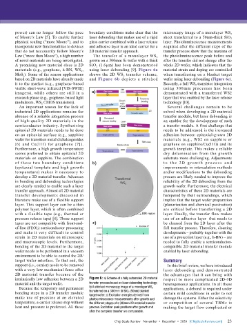
        materials (e.g., graphene, h-BN, WS 2 ,   using laser debonding [9]. Figure 6a   material strain and doping are controlled
        MoS 2 ). Some of the sensor applications   shows the 2D WS 2  transfer scheme,   when transferring on a blanket target
        based on 2D materials have already made   and  Figure 6b depicts a stitched   wafer using laser debonding (Figure 6c).
        it to the market (e.g., graphene-based                                Recently, a full WS 2  transistor integration
        visible short-wave infrared [VIS-SWIR]                                using 300mm processes has been
        imagers), while others are still in a                                 demonstrated with a transferred WS2
        research phase (e.g., graphene-based light                            layer that was enabled by the laser release
        modulators, WS 2  CMOS transistors).                                  technology [10].
          An important reason for the lack of                                   Several challenges remain to be
        industrial 2D applications remains the                                solved when developing a 2D material
        absence of a reliable integration process                             transfer module, but laser debonding is
        of high-quality 2D materials in the                                   an enabler for the development of such
        semiconductor industry. Synthesizing                                  a transfer module. A first challenge that
        epitaxial 2D materials needs to be done                               needs to be addressed is the increased
        on an epitaxial surface (e.g., sapphire                               adhesion between epitaxial-grown 2D
        wafer for transition metal dichalcogenides                            materials (e.g., WS2 on sapphire or
        [6] and Cu(111) for graphene [7]).                                    graphene on sapphire/Cu(111)) and its
        Furthermore, a high growth temperature                                growth template. This makes a reliable
        seems preferred to obtain epitaxial 2D                                dry  delamination from the growth
        materials on sapphire. The combination                                substrate more challenging. Adjustments
        of these two boundary conditions                                      t o t h e 2D g r o w t h p r o c e s s a n d
        (epitaxial template and high growth                                   improvements in intercalation methods
        temperature) makes it necessary to                                    and/or modifications to the debonding
        develop a 2D material transfer. Advances                              process are likely needed to improve the
        in bonding and debonding technologies                                 reliability of the 2D debonding from the
        are clearly needed to enable such a layer                             growth wafer. Furthermore, the electrical
        transfer approach. Almost all 2D material                             characteristics of these 2D materials are
        transfer developments discussed in                                    hampered by their surroundings, which
        literature make use of a flexible support                             implies that the target wafer preparation
        layer. This support layer can be a thin                               (planarization and chemical passivation)
        polymer layer, which is often combined                                are critical before transferring a 2D
        with a flexible tape (e.g., thermal or                                layer. Finally, the transfer flow makes
        pressure release tape) [8]. These support                             use of an adhesive layer  that needs to
        tapes are not compatible with front-end-                              be cleaned from the 2D layer after the
        of-line (FEOL) semiconductor processing                               full transfer process. Therefore, cleaning
        and make it very difficult to control                                 developments – probably together with the
        strain in 2D materials on microscopic                                 use of a protection layer (e.g., h-BN) – are
        and macroscopic levels. Furthermore,                                  needed to fully enable a semiconductor-
        bonding of the 2D material to the target                              compatible 2D material transfer module
        wafer needs to be performed in a vacuum                               enabled by laser debonding.
        environment to be able to control the 2D/
        target wafer interface. To that end, the                              Summary
        support (i.e., carrier) needs to be removed                             In this brief review, we have introduced
        with a very low mechanical force after                                laser debonding and demonstrated
        2D material transfer because of the                                   the advantages that it can bring with
        intrinsically low adhesion between a 2D   Figure 6: a) Scheme of a fully automated 2D material   respect to more complicated 2D-3D
        material and the target wafer.     transfer process based on laser debonding technology;   heterogeneous applications. In all these
          Because the temporary and permanent   b) A stitched microscopy image of a monolayer WS 2    applications, a debond is required under
        bonding steps in a 2D transfer module   transferred on a 300mm Si/SiO 2  (50nm) blanket   certain mild conditions in order to not
        make use of pressure at an elevated   target wafer; c) Excitation energies derived from   damage the systems. Either the selectivity
                                           photoluminescence measurements after growth and
        temperature, a carrier release step without   the different stages of a 300mm 2D material transfer   or competition of several TBMs is
        heat and pressure is preferred. All these   process. Excitation peak positions after growth and   making the target flow complicated or
                                           after the complete transfer are comparable.

                                                                                                             23
                                                       Chip Scale Review   November  •  December  •  2020   [ChipScaleReview.com]  23

