Page 21 - ChipScale_Nov-Dec_2020-digital
P. 21
Laser debonding in 2D and 3D heterogeneous applications


        By Koen Kennes [imec]  Alice Guerrero [Brewer Science]
        T        his article will discuss the


                 i mpact of la ser debond
                 processing for 2D and 3D
                 heterogeneous applications.
        To this end, the fundamentals of laser
        debonding will be introduced. The focus,
        however, will be on highlighting its use
        in several imec programs such as fan-out
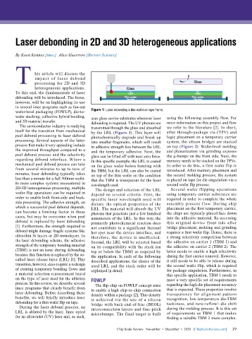
        wafer-level packaging (FOWLP), die-to-  Figure 1: Laser debonding a thin wafer on tape frame.
        wafer stacking, collective hybrid bonding,   uses glass carrier substrates whenever laser   using the following assembly flow. For
        and 2D material transfer.          debonding is required. The UV photons are   more information on this project and flow
          The semiconductor industry is readying   transmitted through the glass and absorbed   we refer to the literature [2]. In short,
        itself for the transition from mechanical   by the LRL (Figure 1). This layer will   after through-package via (TPV) and
        peel debond processing to laser debond   photochemically degrade and break up   logic placement on a temporary carrier
        processing. Several aspects of the latter   into smaller fragments, which will result   system, the silicon bridges are stacked
        process that make it very appealing include   in adhesive strength loss between the LRL   on top (Figure 2). Wafer-level molding
        the improved throughput compared to a   and the temporary adhesive. Next, the   and planarization via grinding exposes
        peel debond process and the selectivity   glass can be lifted off with near zero force.   the µ-bumps on the front side. Next, the
        regarding debond interface. Where a   In this specific example, the LRL is coated   memory needs to be stacked on the TPVs.
        mechanical peel debond process can take   on the glass wafer before bonding with   In order to do this, a first wafer flip is
        from several minutes to up to tens of   the TBM, but the LRL can also be coated   introduced. After memory placement and
        minutes, laser debonding typically takes   on top of the thin wafer on the condition   the second molding process, the system
        less than a minute for a full 300mm wafer.   that the TBM is transparent for the laser   is placed on tape for die singulation via a
        In more complex systems encountered in   wavelength used.             second wafer flip process.
        2D-3D heterogeneous processing, multiple   The design and selection of the LRL   Several wafer flipping operations
        wafer flip operations can be required in   depend on several criteria. First, the   using temporary carrier substrates are
        order to enable both front-side and back-  specific laser wavelength used will   required in order to complete the whole
        side processing. The adhesive strength, on   dictate the optical properties of the   assembly process flow. During chip
        which a successful peel debond depends,   LRL. The material will absorb the UV   placement on the first temporary carrier,
        can become a limiting factor in these   photons that penetrate just a few hundred   the chips are typically placed face down
        cases, but may be overcome when peel   nanometers of the LRL. In this way, the   into the adhesive material. Re-accessing
        debond is replaced by laser debonding   primarily photochemical reaction does   this original device front side after
        [1]. Furthermore, the strength required to   not contribute to a significant thermal   bridge placement, molding and grinding
        debond might damage fragile systems like   hot spot near the device interface, and   requires a first wafer flip. Hence, there is
        ultra-thin Si layers or 2D monolayers. In   therefore, the device is unaffected.   a strong selectivity competition between
        the laser debonding scheme, the adhesive   Second, the LRL will be selected based   the adhesive on carrier 1 (TBM 1) and
        strength of the temporary bonding material   on its compatibility with the stack (on   the adhesive on carrier 2 (TBM 2). The
        (TBM) is not an issue during debonding   top or below the TBM) as required by   latter needs to enable a high selectivity
        because this function is replaced by the so-  the application. In each of the following   during the first carrier removal. However,
        called laser release layer (LRL) [1]. This   described applications, the choice of the   it still needs to be able to release during
        transition, however, does require a redesign   used LRL and the stack order will be   the second wafer flip, which is required
        of existing temporary bonding flows and   explained in detail.        for package singulation. Furthermore, in
        a material selection reassessment based                               this specific application, TBM 1 needs to
        on the type of laser used for the ablation   FOWLP                    meet a very specific set of requirements
        process. In this review, we describe several   The flip-chip on FOWLP concept aims   regarding the high die placement accuracy
        imec programs that clearly benefit from   to enable a high chip-to-chip connection   that is expected. These properties involve
        laser debonding. Before describing these   density within a package [2]. This density   transparency for alignment pattern
        benefits, we will briefly introduce laser   is achieved via the use of a silicon   recognition, low temperature die-TBM
        debonding for a thin wafer flip on tape.  bridge with back-end-of-line (BEOL)   tackiness, and zero-reflow/–die shift
          During the laser debond process, an   interconnection layers and fine-pitch   during the molding process. It is this set
        LRL is ablated by the laser. Imec opted   microbumps. The final target is built   of requirements on TBM 1 that makes
        for an ultraviolet (UV) laser and, as such,                           finding a suitable TBM 2 more complex.

                                                                                                             19
                                                       Chip Scale Review   November  •  December  •  2020   [ChipScaleReview.com]  19

