Page 18 - ChipScale_Nov-Dec_2020-digital
P. 18
different nodes for cost and technology   is much easier, but the heat from the   the very costly matrix multiplication
        optimization; and 2) die disaggregation:   accelerator must escape upward through   operation, which dominates DN N
        allowing higher yielding and lower   the memor y, posing a signif icant   computation, can be done in a single
        cost smaller dies that can be flexibly   thermal challenge.           step exactly where the weights are
        combined. The most common example    In the long term, heterogeneous   stored, without having to move them
        of  heterogeneous  integration  in  AI   integration can help facilitate two other   from memory to the processor. Such
        today is the use of the Si interposer   possibilities related to analog-based   accelerators,  with  different  process
        for connectivity between a GPU or AI   elements. In the first of these, the analog   requirements because of the analog
        accelerator and 3D-stacked HBM. A   elements  are  used  as  high-density   elements, are likely to be fabricated
        noteworthy research example of die   memory elements, enabling much higher   in a technology different from other
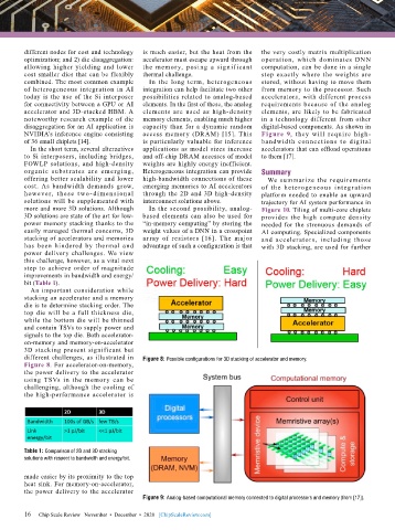
        disaggregation for an AI application is   capacity than for a dynamic random   digital-based components. As shown in
        NVIDIA’s inference engine consisting   access memory (DRAM) [15]. This   Figure 9, they will require high-
        of 36 small chiplets [14].         is particularly valuable for inference   bandwidth connections to digital
          In the short term, several alternatives   applications as model sizes increase   accelerators that can offload operations
        to Si interposers, including bridges,   and off-chip DRAM accesses of model   to them [17].
        FOWLP solutions, and high-density   weights are highly energy inefficient.
        organic  substrates  are emerging,   Heterogeneous integration can provide   Summary
        offering better scalability and lower   high-bandwidth connections of these   We summarize the requirements
        cost. As bandwidth demands grow,   emerging memories to AI accelerators   of the heterogeneous integration
        however,  these  t wo - di mensional   through the 2D and 3D high-density   platform needed to enable an upward
        solutions will be supplemented with   interconnect solutions above.   trajectory for AI system performance in
        more and more 3D solutions. Although   In the second possibility, analog-  Figure 10. Tiling of multi-core chiplets
        3D solutions are state of the art for low-  based elements can also be used for   provides the high compute density
        power memory stacking thanks to the   “in-memory computing” by storing the   needed for the strenuous demands of
        easily managed thermal concerns, 3D   weight values of a DNN in a crosspoint   AI computing. Specialized components
        stacking of accelerators and memories   array of resistors  [16]. The  major   and accelerators, including those
        has been hindered by thermal and   advantage of such a configuration is that   with 3D stacking, are used for further
        power delivery challenges. We view
        this challenge, however, as a vital next
        step to achieve order of magnitude
        improvements in bandwidth and energy/
        bit (Table 1).
          An important consideration while
        stacking an accelerator and a memory
        die is to determine stacking order. The
        top die will be a full thickness die,
        while the bottom die will be thinned
        and contain TSVs to supply power and
        signals to the top die. Both accelerator-
        on-memory and memory-on-accelerator
        3D stacking present significant but
        different challenges, as illustrated in   Figure 8: Possible configurations for 3D stacking of accelerator and memory.
        Figure 8. For accelerator-on-memory,
        the power delivery to the accelerator
        using TSVs in the memory can be
        challenging, although the cooling of
        the high-performance accelerator is


        Table 1: Comparison of 2D and 3D stacking
        solutions with respect to bandwidth and energy/bit.

        made easier by its proximity to the top
        heat sink. For memory-on-accelerator,
        the power delivery to the accelerator
                                           Figure 9: Analog-based computational memory connected to digital processors and memory (from [17]).

        16   Chip Scale Review   November  •  December  •  2020   [ChipScaleReview.com]
        16

