Page 14 - ChipScale_Nov-Dec_2020-digital
P. 14
a s d e e p t r e n c h   In the case of organic interposers,
                                                            capa cit or s ( DT   the dielectric materials used for the
                                                            caps) or inductors.   finer surface layers do not have this
                                                            T h i s  s i l i c o n   tremendous difference in the CTE as
                                                            i n t er p o s er  h a s   compared to the underlying organic
                                                            TSVs that allow   package. The silicon die attached to the
                                                            for communication   top side of the fine layers are generally
                                                            b e t w e en  t h e   smaller than a single reticle size (~26mm
                                                            e nt it ie s  o n t h e   x 32mm), so there is no instance of a large
                                                            opposing surfaces,   piece of silicon (2x reticle size or larger)
                                                            as well as surface   attached to an organic substrate, as in the
                                                            w i r i ng t h a t   case of the silicon interposer.
                                                            may be built in
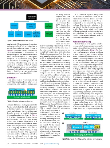
        Figure 3: Heterogeneous integration options.
                                                            dielectric f ilms   Redistribution wiring
        requirements. Heterogeneous integration             such as oxides,     Redistribution wiring that enables
        options are classified as belonging to   thereby enabling connectivity between   connectivity between components can be
        one of three primary types shown in   components placed on the same side of   made using either inorganic dielectrics
        Figure 3: interposer, redistribution wiring,   the interposer. Silicon interposers are   or organic dielectrics. Figure 5a shows
        and three-dimensional (3D) integration. The   completely compatible with standard   two  configurations  where  a  silicon
        interposer option can further be classified   fabrication processing, but they also   bridge connects two or more chips.
        into a silicon interposer and an organic   have manufacturing costs that stem from   Many varieties of bridges are seen in the
        interposer. The redistribution wiring option   builds in wafer fabrication lines.  literature, including bridges on the surface
        can be either a silicon bridge with back   On the other hand, organic interposers   of the packaging substrate, bridges that
        end of line (BEOL) wiring or a fan-out   are fabricated in laminate manufacturing   are embedded inside the packaging
        wafer-level packaging (FOWLP) option.   companies; they build on the existing   substrate, and bridges that are placed in a
        The 3D integration option has several sub-  organic laminate structures by adding   recess or trench on the top surface of the
        categories, but in all these, the key common   finer surface structures that allow   packaging substrate. This bridge typically
        factor is that there are active dies that   for superior connectivity between   uses inorganic inter-level dielectric
        contain through-silicon vias (TSVs).   components on the top side of the   materials and copper wiring fabricated by
                                           interposer [10]. And they already have   traditional silicon fabrication processes.
        Interposers                        through-vias that enable electrical   A bridge is generally a passive entity
          An interposer is fundamentally an   connection to the other side, thereby   without active logic functionality. It may
        entity that is placed (or interposed)   enabling signal and power transmission.  use a surface dielectric material such
        between two other entities—in this case,   A silicon interposer may fall short of   as oxide, which has a relative dielectric
                                           AI requirements because of its limited   permeability “k” of around 4, or other
                                           scalability. Although a 2x reticle size has   materials with k<4. When k is low, the
                                           been practiced routinely, and 3x reticle   transmission of signals in the embedded
                                           sizes are being offered, the larger the   copper wiring is superior. However, these
                                           interposer gets, the more the potential   materials are typically more fragile and
                                           for stress-related issues. When silicon   less robust than silicon oxides and may
                                           interposers are joined to organic packaging   cause reliability issues during the life of
                                           substrates, there is differential expansion   the component. The advantage of silicon
        Figure 4: Classical packaging configuration.  and contraction between them because of   bridge technology is very fine lines
        a silicon chip and a packaging substrate.   differences in the coefficients of thermal   and spacings, leading to a rich density
        An important attribute of all interposers   expansion (CTE); the silicon interposer   of transmission lines connecting the
        is that they enable the transmission of   CTE is around 2.6ppm/ºC, whereas that   chips. However, bridges are physically
        electrical signals through them and   of the organic substrate is
        thereby provide a conduit between   12-17ppm/ºC. Differential
        silicon and package, as shown in Figure   expansion and contraction
        4. A silicon interposer is therefore a   create st resses i n the
        passive entity that may have on one   assembly, including stresses
        surface, one or more chips joined to it   in the interconnections, and
        by solder or copper interconnects, while   the surfaces to which they
        on the opposing surface it may be joined   are joined. As the silicon
        to a packaging substrate with solder   gets larger in size, there are
        interconnects. Additionally, it may   larger shear stresses in the
        have passive elements like capacitors,   interconnects at the extreme
        resistors, and/or inductors joined to   edges, which may create
        either or both surfaces. It may also   manufacturability, as well as
        contain built-in passive elements, such   reliability concerns.
                                                                   Figure 5: Example(s) of: a) Bridges; b) Fan-out wafer-level packaging.

        12
        12   Chip Scale Review   November  •  December  •  2020   [ChipScaleReview.com]

