Page 16 - ChipScale_Nov-Dec_2020-digital
P. 16
juxtaposed in the narrow space between   vertically,  and  communicate  with   because copper has among the lowest
        neighboring die, which limits the area   each other using TSVs as shown in    resistivities of all materials compatible
        of connection to the edges of the chips     Figure 6. The power of 3D integration   with silicon fab processing. The copper
        being connected.                   lies in its ability to provide relatively   TSV integration must necessarily occur
          Redistribution wiring may also   shor t z-direction communication   after the FEOL is completed because
        be achieved using organic dielectric   channels, and to avoid longer x-y   of the high-temperature processing
        materials and copper wiring; this allows   travel between chips, thereby avoiding   in the FEOL, which copper is unable
        for superior connectivity between   su sce pt ibi l it y  t o  c ross  t al k  a nd   to withstand. The TSV is therefore
        chips on the substrate (Figure 5b).   insertion loss, both of which impede   integrated during the BEOL fabrication
        This category is also known as fan-out   pe r f o r ma n c e .  3 D
        wafer-level packaging (WLP) in one   integration can therefore
        manifestation. The key idea is to use   create tight coupling with
        known good die (KGD) and connect   very high bandwidth. In
        them using copper wiring in a polymer   the case of accelerator
        (organic dielectric). This connection may   to memory connections,
        be done by using KGD, placing them   such a coupling enables
        on a temporary carrier with an adhesive   the accelerator to have
        layer, then covering them in a molding   rapid access to memory
        compound, grinding down the mold to   a t  v e r y  l o w e n e r g y
        reveal their contact pads, and finally   c os t .  T h is  c o up l i n g
        creating redistribution wiring. Examples   m a y b e e n h a n c e d
        of organic redistribution layer wiring are   further if the die to die
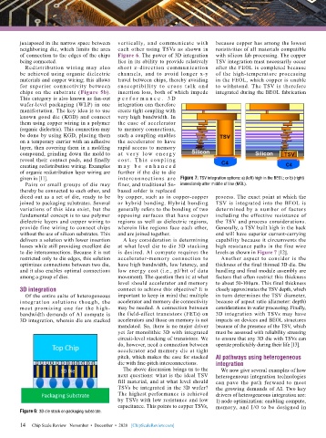
        given in [11].                     i ntercon nect ions a re  Figure 7: TSV integration options: a) (left) high in the BEOL; or b) (right)
          Pairs or small groups of die may   finer, and traditional Sn-  immediately after middle of line (MOL).
        thereby be connected to each other, and   based solder is replaced
        diced out as a set of die, ready to be   by copper, such as in copper-copper   process. The exact point at which the
        joined to packaging substrates. Several   or hybrid bonding. Hybrid bonding   TSV is integrated into the BEOL is
        variations of this idea exist, but the   generally refers to the bonding of two   determined by a number of factors
        fundamental concept is to use polymer   opposing surfaces that have copper   including the effective resistance of
        dielectric layers and copper wiring to   regions as well as dielectric regions,   the TSV and process considerations.
        provide fine wiring to connect chips   wherein like regions face each other,   Generally, a TSV built high in the back
        without the use of silicon substrates. This   and are joined together.  end will have superior current-carrying
        delivers a solution with lower insertion   A key consideration is determining   capability because it circumvents the
        losses while still providing excellent die   at what level die to die 3D stacking   high resistance paths in the fine wire
        to die interconnections. Because it is not   is desired. AI compute requires the   levels as shown in Figure 7 [12].
        restricted only to die edges, this solution   accelerator-memory connection to   Another aspect to consider is the
        optimizes connections between two die,   have high bandwidth, low latency, and   thickness of the final thinned 3D die. Die
        and it also enables optimal connections   low energy cost (i.e., pJ/bit of data   handling and final module assembly are
        among a group of dies.             movement). The question then is: at what   factors that often restrict this thickness
                                           level should accelerator and memory   to about 50-100µm. This final thickness
        3D integration                     connect to achieve this objective? It is   closely approximates the TSV depth, which
          Of the entire suite of heterogeneous   important to keep in mind that multiple   in turn determines the TSV diameter,
        integration solutions though, the   accelerator and memory die connectivity   because of aspect ratio (diameter: depth)
        most promising one for the high-   may be needed. A connection between   considerations in wafer processing. Finally,
        bandwidth demands of AI compute is   the field-effect transistors (FETs) on   3D integration with TSVs may have
        3D integration, wherein die are stacked   accelerators and those on memory is not   impacts on devices and BEOL structures
                                           mandated. So, there is no major driver   because of the presence of the TSV, which
                                           yet for monolithic 3D with integrated   must be assessed with reliability stressing
                                           circuit-level stacking of transistors. We   to ensure that any 3D die with TSVs can
                                           do, however, need a connection between   operate predictably during their life [13].
                                           accelerator and memory die at tight
                                           pitch, which makes the case for stacked   AI pathways using heterogeneous
                                           die with fine-pitch interconnections.  integration
                                             The above discussion brings us to the   We now give several examples of how
                                           next questions: what is the ideal TSV   heterogeneous integration technologies
                                           fill material, and at what level should   can pave the path forward to meet
                                           TSVs be integrated in the 3D wafer?   the growing demands of AI. Two key
                                           The highest performance is achieved   drivers of heterogeneous integration are:
                                           by TSVs with low resistance and low   1) node optimization: enabling compute,
                                           capacitance. This points to copper TSVs,   memory,  and  I/O  to  be  designed  in
        Figure 6: 3D die stack on packaging substrate.

        14
        14   Chip Scale Review   November  •  December  •  2020   [ChipScaleReview.com]

