Page 22 - ChipScale_Nov-Dec_2020-digital
P. 22
silicon vias (TSVs) and microbump pitches.
                                                                              Implementing such fine-pitch microbumps
                                                                              for multi-die stacking requires a careful
                                                                              assembly process to prevent any damage to
                                                                              the tiny microbumps. In this study, a glass
                                                                              carrier is bonded to the bump side of the
                                                                              wafer followed by mechanically debonding
                                                                              the silicon carrier and mounting the front
                                                                              side on tape. At the end of the assembly
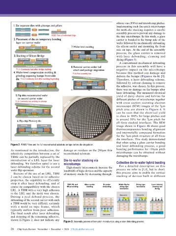
                                                                              process, the glass carrier is removed
                                                                              with laser debonding, cleaning and
                                                                              dicing (Figure 3).
                                                                                A conventional mechanical debonding
                                                                              process in this assembly will have a
                                                                              negative impact on the microbumps
                                                                              because this method can damage and
                                                                              deform the bumps (Figures 4a-b) [3].
                                                                              Therefore, a laser debonding scheme,
                                                                              followed by solvent cleaning to remove
                                                                              the adhesive, was chosen. In this process,
                                                                              there was no damage on the bumps after
                                                                              laser debonding. The measured electrical
                                                                              yield of daisy chains and kelvins for
                                                                              different pitches of microbumps together
                                                                              with cross section scanning electron
                                                                              microscope (SEM) images of the 7µm
                                                                              pitch area are shown in Figure 4. It
                                                                              can be seen that the electrical yield
                                                                              is close to 100% for large pitches and
                                                                              is around 50% for the 7µm pitch for
                                                                              all three stacked interfaces. The SEM
                                                                              image shown in Figure 4b shows good
                                                                              thermocompression bonding alignment
                                                                              and intermetallic compound formation
                                                                              for the 7µm pitch structure at all three
                                                                              die interfaces. This study demonstrated
                                                                              that when using a glass carrier bonding
        Figure 2: FOWLP flow and the full reconstructed substrate on tape before die-singulation.  and laser debonding process, a good

        As mentioned in the introduction, the   damage or residues on the 200µm thin   bonding performance for <10µm pitch
        selectivity competition between a set of   reconstituted substrate.   microbumps can be obtained without
        TBMs can be partially replaced by the                                 damaging the microbumps.
        introduction of a LRL layer for laser   Die-to-wafer stacking via
        debonding. We therefore opted to use a   microbumps                   Collective die-to-wafer hybrid bonding
        laser debonding scheme for the second   High-density interconnects increase the   For a detailed description on this
        wafer flip operation.              bandwidth of logic devices and the capacity   process we refer to [1,4], but in short:
          Because of the use of an LRL, TBM   of memory stacks by decreasing through-  this process aims to enable the vertical
        2 can be chosen based on its adhesive                                 stacking of devices built in different
        properties, the capability to efficiently
        strip it after laser debonding, and of
        course its compatibility with the chosen
        LRL. A TBM with a very high adhesion
        to the LRL and the mold was chosen.
        During a peel debond process, the
        debonding of the second carrier with such
        a TBM would be very difficult, certainly
        with a mold on tape frame, which
        typically suffers from poor adhesion.
        The final result after laser debonding
        and stripping of the remaining adhesive,
        shown in Figure 2, does not indicate any
                                           Figure 3: Assembly process of fine-pitch microbumps using a laser debonding process.

        20
        20   Chip Scale Review   November  •  December  •  2020   [ChipScaleReview.com]

