Page 24 - ChipScale_Nov-Dec_2020-digital
P. 24
Figure 4: a) An optical image shows damaged
        microbumps <10µm after mechanical peel
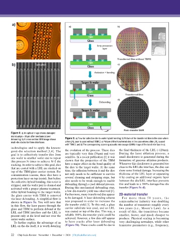
        debonding; b) A cross section SEM image shows   Figure 5: a) Flow for collective die-to-wafer hybrid bonding; b) Picture of the transferred dies in the case where
        multi-die stacks for three interfaces.  a thin LRL layer is used without TBM 2; c) Picture of the transferred dies in the case where a thin LRL is used
                                           with TBM 2; and d) The corresponding scanning acoustic microscope (SAM) image of the bond interface in c).
        technologies and to apply the known-
        good-die selection method [1,4]. The   the evolution of the process. These dies   the final thickness of the LRL (~120nm).
        goal is to collectively transfer dies from   are typically very thin (50µm) and very   During the laser ablation process, a
        one wafer to another wafer and to repeat   sensitive. In a recent publication [1] it was   small shockwave is generated during the
        this process N times to achieve N>2 die   shown that the properties of the TBM   formation of gaseous ablation products.
        stacking. In order to achieve this goal, dies   have a major effect on the bond quality of   Whenever this shockwave is generated too
        that are coated with a LRL are stacked on   the dies to the target wafer. At the same   close to the LRL/die interface, the dies can
        top of the TBM/glass carrier system. For   time, the adhesion between it and the dies   show some limited damage. Increasing the
        contamination reasons, these dies have a   not only needs to be sufficient to survive   thickness of the LRL layer or separating
        protection layer on top (resist). Just before   several cleaning and stripping steps, but   it by coating an additional organic layer
        the collective hybrid bonding, this resist is   also needs to be weak enough to enable   between the die/LRL interface prevents
        stripped, and the wafer pair is cleaned and   debonding through a peel debond process.   this and leads to a 100% damage-free die
        activated with a proper plasma treatment.   During this mechanical debonding step,   transfer (Figure 5c-d).
        After hybrid bonding to the target wafer,   a low die-transfer yield was observed [4].
        the glass carrier with TBM is removed   Furthermore, many transferred dies appear   2D-material transfer
        via laser debonding. A simplified flow is   to be damaged. A laser debonding scheme   Fo r m o r e t h a n 5 0 y e a r s , t h e
        shown in Figure 5a. You will note that   was proposed in order to increase the   semiconductor industry was doubling
        in this flow, the laser passes through the   die transfer yield [1]. To this end, a glass   the number of transistors roughly every
        glass and TBM to perform debond at the   carrier substrate was used, and an LRL   two years (i.e., Moore’s Law). As a
        LRL and TBM interface and the LRL is   was coated on top of the dies. This way, a   result of this, the transistors became
        present only at die level and not over the   reliable 100% die-transfer yield could be   smaller, faster, and much cheaper to
        entire wafer surface.              achieved. However, a few dies still appear   produce. Physical scaling is becoming
          To further explain the advantage of an   to have cracks after laser debonding   very challenging nowadays, while other
        LRL on the die itself, it is worth detailing   (Figure 5b). These cracks could be due to   transistor parameters (e.g., frequency,

        22   Chip Scale Review   November  •  December  •  2020   [ChipScaleReview.com]
        22

