Page 27 - ChipScale_Nov-Dec_2020-digital
P. 27
Chip-scale power transistor packaging


        By Shaun Bowers [Amkor Technology, Inc.]
        E        xpanding applications for


                 advanced power packaging
                 have created the need for new
                 package design concepts to
        fill the gaps between existing discrete and
        power module designs. The integrated
        power market continues to expand and
        evolve with established and advanced
        power semiconductor technologies.
        Understanding the current environment
        and the challenges of moving forward are
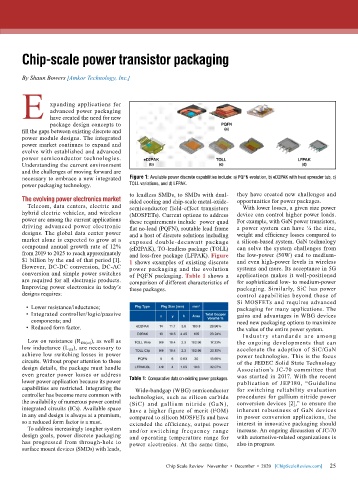
        necessary to embrace a new integrated   Figure 1: Available power discrete capabilities include: a) PQFN evolution, b) eD2PAK with heat spreader tab, c)
        power packaging technology.        TOLL variations, and d) LFPAK.
                                           to leadless SMDs, to SMDs with dual-  they have created new challenges and
        The evolving power electronics market  sided cooling and chip-scale metal-oxide-  opportunities for power packages.
          Telecom, data centers, electric and   semiconductor field-effect transistors   With lower losses, a given size power
        hybrid electric vehicles, and wireless   (MOSFETs). Current options to address   device can control higher power loads.
        power are among the current applications   these requirements include  power quad   For example, with GaN power transistors,
        driving advanced power electronic   flat no-lead (PQFN), routable lead frame   a power system can have ¼ the size,
        designs. The global data center power   and a host of discrete solutions including   weight and efficiency losses compared to
        market alone is expected to grow at a   exposed double-decawatt package   a silicon-based system. GaN technology
        compound annual growth rate of 12%   (eD2PAK), TO-leadless package (TOLL)   can solve the system challenges from
        from 2019 to 2025 to reach approximately   and loss-free package (LFPAK). Figure   the low-power (50W) end to medium-
        $1 billion by the end of that period [1].   1 shows examples of existing discrete   and even high-power levels in wireless
        However, DC-DC conversion, DC-AC   power packaging and the evolution   systems and more. Its acceptance in 5G
        conversion and simple power switches   of PQFN packaging. Table 1 shows a   applications makes it well-positioned
        are required for all electronic products.   comparison of different characteristics of   for sophisticated low- to medium-power
        Improving power electronics in today’s   these packages.              packaging. Similarly, SiC has power
        designs requires:                                                     control capabilities beyond those of
                                                                              Si MOSFETs and requires advanced
          •  Lower resistance/inductance;                                     packaging for many applications. The
          •  Integrated controller/logic/passive                              gains and advantages in WBG devices
           components; and                                                    need new packaging options to maximize
          •  Reduced form factor.                                             the value of the entire power system.
                                                                                I ndu st r y st a nd a rd s a re a mong
          Low on resistance (R DS(on) ), as well as                           the ongoing developments that can
        low inductance (L DS ), are necessary to                              accelerate the adoption of SiC/GaN
        achieve low switching losses in power                                 power technologies. This is the focus
        circuits. Without proper attention to these                           of the JEDEC Solid State Technology
        design details, the package must handle                               Association’s JC-70 committee that
        even greater power losses or address                                  was started in 2017. With the recent
        lower power application because its power   Table 1: Comparative data on existing power packages.  publication of JEP180, “Guideline
        capabilities are restricted. Integrating the   Wide-bandgap (WBG) semiconductor   for switching reliability evaluation
        controller has become more common with   technologies, such as silicon carbide   procedures for gallium nitride power
        the availability of numerous power control   (SiC) and gallium nitride (GaN),   conversion devices [2],” to ensure the
        integrated circuits (ICs). Available space   have a higher figure of merit (FOM)   inherent robustness of GaN devices
        in any end design is always at a premium,   compared to silicon MOSFETs and have   in power conversion applications, the
        so a reduced form factor is a must.  extended the efficiency, output power   interest in innovative packaging should
          To address increasingly tougher system   and/or switching frequency range   increase. An ongoing discussion of JC-70
        design goals, power discrete packaging   and operating temperature range for   with automotive-related organizations is
        has progressed from through-hole to   power electronics. At the same time,   also in progress.
        surface mount devices (SMDs) with leads,

                                                                                                             25
                                                       Chip Scale Review   November  •  December  •  2020   [ChipScaleReview.com]  25

