Page 31 - ChipScale_Nov-Dec_2020-digital
P. 31
Low- to mid-power integration using the PCSP concept
          There is a strong movement towards integration within the
        power market—and power density plays a big part in the adoption
        of various integration methods. In the low- to mid-power range,
        integration can involve different methods depending on the use
        case and the original package format.
          Three basic approaches outline different paths to integration.
        One is to simply include the controller and MOSFET devices into
        a split-pad lead frame, or PQFN. This is common, but limited as
        far as power and performance  are concerned and options to add
        passive elements are typically done off-package. Another is to
        include more exotic materials within the molded interface such
        as direct bonded copper (DBC), which is common in insulated-
        gate bipolar transistor (IGBT) modules. Last, there are efforts
        to directly embed the MOSFET dice into a laminate substrate
        or redistribution layer (RDL) package. Although the embedded
        option has merit in mid-power options, supply chain issues have
        historically slowed widespread adoption of a fully-embedded
        option. Each of these integration paths has advantages and
        disadvantages, but share a few common traits. They all attempt
        to maximize the contact area to the source and drain of the FET,
        put as much conductive material as possible within the module,
        and design a reduced electrical path for successful integration.
          An approach to integration that uses PCSP technology might
        resolve some of the fundamental issues inherent in the other
        approaches. Starting with a common form factor and integrating
        this approach into more mainstream module aspects will allow
        for wider adoption. Allowing the MOSFET(s) to be pre-packaged
        allows for individual or gang testing, therefore it can be treated
        as known good die (KGD) for improved yield. Mounting a
        package directly to a substrate and PCB may reduce the overall
        complexity and cost.
          The modular approach should also enhance the performance of
        the overall system because of some specific design options for the
        integrated device. Signal paths directly to the PCB will maintain
        low resistance/inductance. Using a high-density but small form
        factor package allows thick Cu interfaces only in areas critical
        to the design. Also, critical components and devices can be
        distance-optimized for performance and cost. By applying this
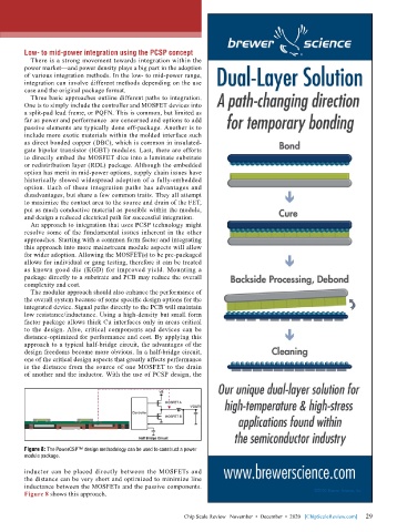
        approach to a typical half-bridge circuit, the advantages of the
        design freedoms become more obvious. In a half-bridge circuit,
        one of the critical design aspects that greatly affects performance
        is the distance from the source of one MOSFET to the drain
        of another and the inductor. With the use of PCSP design, the


        Figure 8: The PowerCSP™ design methodology can be used to construct a power
        module package.

        inductor can be placed directly between the MOSFETs and
        the distance can be very short and optimized to minimize line
        inductance between the MOSFETs and the passive components.
        Figure 8 shows this approach.


                                                                                                             29
                                                       Chip Scale Review   November  •  December  •  2020   [ChipScaleReview.com]  29

