Page 32 - ChipScale_Nov-Dec_2020-digital
P. 32
efficiency and lower noise. A patent has
                                                                              been filed for this design approach.
                                                                                T h e  l ow - p owe r  m a r k e t ,  l i k e
                                                                              smartphones, has already implemented
                                                                              wafer-level CSP MOSFETs. This mounting
                                                                              of a power transistor directly to the mother
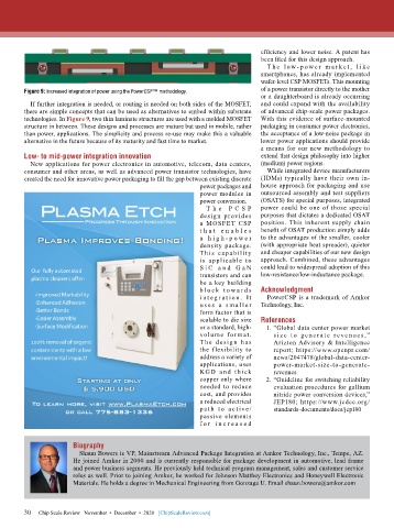
        Figure 9: Increased integration of power using the PowerCSP™ methodology.
                                                                              or a daughterboard is already occurring
          If further integration is needed, or routing is needed on both sides of the MOSFET,   and could expand with the availability
        there are simple concepts that can be used as alternatives to embed within substrate   of advanced chip-scale power packages.
        technologies. In Figure 9, two thin laminate structures are used with a molded MOSFET   With this evidence of surface-mounted
        structure in between. These designs and processes are mature but used in mobile, rather   packaging in consumer power electronics,
        than power, applications. The simplicity and process re-use may make this a valuable   the acceptance of a low-noise package in
        alternative in the future because of its maturity and fast time to market.  lower power applications should provide
                                                                              a means for our new methodology to
        Low- to mid-power integration innovation                              extend that design philosophy into higher
          New applications for power electronics in automotive, telecom, data centers,   (medium) power regions.
        consumer and other areas, as well as advanced power transistor technologies, have   While integrated device manufacturers
        created the need for innovative power packaging to fill the gap between existing discrete   (IDMs) typically have their own in-
                                                            power packages and   house approach for packaging and use
                                                            power modules in   outsourced assembly and test suppliers
                                                            power conversion.  (OSATS) for special purposes, integrated
                                                              T h e  P C S P   power could be one of those special
                                                            design  provides   purposes that dictates a dedicated OSAT
                                                            a MOSFET CSP      position. This inherent supply chain
                                                            t h a t  en a b l es   benefit of OSAT production simply adds
                                                            a  h i g h - p owe r   to the advantages of the smaller, cooler
                                                            density  package.   (with appropriate heat spreader), quieter
                                                            T h is capabilit y   and cheaper capabilities of our new design
                                                            is applicable to   approach. Combined, these advantages
                                                            S i C  a n d  G a N   could lead to widespread adoption of this
                                                            transistors and can   low-resistance/low-inductance package.
                                                            be a key building
                                                            b l o c k   t o w a r d s   Acknowledgment
                                                            i n t e g r a t i o n .  I t   PowerCSP is a trademark of Amkor
                                                            u s e s a s m a l l e r   Technology, Inc.
                                                            form factor that is
                                                            scalable to die size   References
                                                            or a standard, high-  1.  “Global data center power market
                                                            volu me for mat.      si z e  t o  gen e r a te  r e venu e s ,”
                                                            T he  de sig n  ha s   Arizton Advisory & Intelligence
                                                            the flexibility to    report; https://www.openpr.com/
                                                            address a variety of   news/2047478/global-data-center-
                                                            applications, uses    power-market-size-to-generate-
                                                            KGD a nd t h ick      revenues
                                                            copper only where   2.  “Guideline for switching reliability
                                                            needed to reduce      evaluation procedures for gallium
                                                            cost, and provides    nitride power conversion devices,”
                                                            a reduced electrical   JEP180; https://www.jedec.org/
                                                            p a t h t o a c t ive /  standards-documents/docs/jep180
                                                            passive elements
                                                            f o r  i n c r e a s ed


                       Biography
                         Shaun Bowers is VP, Mainstream Advanced Package Integration at Amkor Technology, Inc., Tempe, AZ.
                       He joined Amkor in 2000 and is currently responsible for package development in automotive, lead frame
                       and power business segments. He previously held technical program management, sales and customer service
                       roles as well. Prior to joining Amkor, he worked for Johnson Matthey Electronics and Honeywell Electronic
                       Materials. He holds a degree in Mechanical Engineering from Gonzaga U. Email shaun.bowers@amkor.com


        30   Chip Scale Review   November  •  December  •  2020   [ChipScaleReview.com]
        30

