Page 42 - ChipScale_Sep-Oct_2020-digital
P. 42

Figure 6: A 30mm die-to-die bonded assembly.


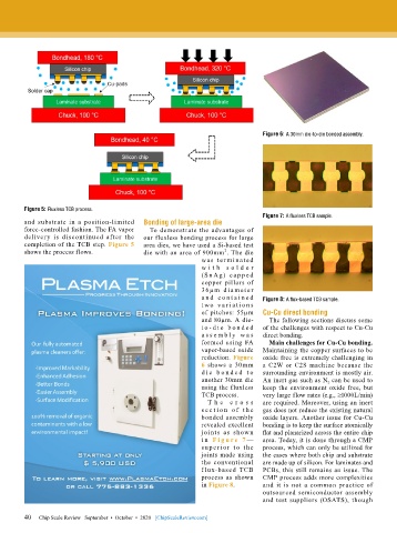
        Figure 5: Fluxless TCB process.
                                                                              Figure 7: A fluxless TCB sample.
        and substrate in a position-limited   Bonding of large-area die
        force-controlled fashion. The FA vapor   To demonstrate the advantages of
        delivery  is  discontinued  after  the   our fluxless bonding process for large
        completion of the TCB step. Figure 5   area dies, we have used a Si-based test
        shows the process flows.           die with an area of 900mm . The die
                                                                   2
                                                            was ter m i nated
                                                            w i t h  s o ld e r
                                                            (S n A g)  c a p p e d
                                                            copper pillars of
                                                            36µ m d ia me t e r
                                                            a n d  co n t ai n e d   Figure 8: A flux-based TCB sample.
                                                            t wo  v a r i at i o n s
                                                            of pitches: 55µm   Cu-Cu direct bonding
                                                            and 80µm. A die-    The following sections discuss some
                                                            to - d i e   b o n d e d   of the challenges with respect to Cu-Cu
                                                            as s e m b l y  w as   direct bonding.
                                                            formed using FA     Main challenges for Cu-Cu bonding.
                                                            vapor-based oxide   Maintaining the copper surfaces to be
                                                            reduction. Figure   oxide free is extremely challenging in
                                                            6  shows  a  30mm   a C2W or C2S machine because the
                                                            d i e b o n d e d t o   surrounding environment is mostly air.
                                                            another 30mm die   An inert gas such as N 2  can be used to
                                                            using the fluxless   keep the environment oxide free, but
                                                            TCB process.      very large flow rates (e.g., ≥1000L/min)
                                                              T h e  c r o s s   are required. Moreover, using an inert
                                                            s e c t i o n o f t h e   gas does not reduce the existing natural
                                                            bonded assembly   oxide layers. Another issue for Cu-Cu
                                                            revealed excellent   bonding is to keep the surface atomically
                                                            joints as shown   flat and planarized across the entire chip
                                                            i n  F i g u r e 7 —  area. Today, it is done through a CMP
                                                            s up e r ior t o t he   process, which can only be utilized for
                                                            joints made using   the cases where both chip and substrate
                                                            the conventional   are made up of silicon. For laminates and
                                                            f lux-based TCB   PCBs, this still remains an issue. The
                                                            process as shown   CMP process adds more complexities
                                                            in Figure 8.      and it is not a common practice of
                                                                              outsourced semiconductor assembly
                                                                              and  test  suppliers  (OSATS),  though

        40
        40   Chip Scale Review   September  •  October  •  2020   [ChipScaleReview.com]
   37   38   39   40   41   42   43   44   45   46   47