Page 43 - ChipScale_Sep-Oct_2020-digital
P. 43
foundries use this process regularly   contact after plating also makes a huge   mounted shroud successfully reduces
        for chip manufacturing. Currently, it   difference because it makes the grain   the surface copper oxides by creating
        makes more sense to mainly rely on   size larger and the copper more ductile.  a reducing mini-environment. FA
        foundries to provide the samples for     Cu-Cu bonding with in situ oxide   vapors react with Cu surface oxides to
        direct Cu-Cu bonding.              reduct ion. We have extensively    create a copper formate layer, which
          Another less explored method is   investigated the effectiveness of the   is eventually decomposed by elevating
        the fly-cutting to planarize the Cu-  FA vapor-based in situ copper oxide   the temperature above 180°C. The Cu-
        surfaces and it results in reasonably flat   reduction process and it is found to be   surface roughness dictates a key TCB
        surfaces (e.g., 10-20nm) in comparison   equally effective for the elimination of   process parameter: bonding pressure.
        with CMP, which can result in ≤1nm   copper oxides. Our FA vapor delivery   We have developed direct Cu-Cu TCB
        surface  roughness.  This  means  that   system along with the bond head   processes for a variety of surface finishes
        we would require very large pressures
        to flatten the asperities on a copper
        surface. Developing a cost-effective
        method to achieve a CMP-like surface
        finish still remains a challenge. The
        f latness requirement becomes even
        more stringent as the die areas, and
        consequently, the total I/O contact area
        sizes, increase. Rougher surfaces would
        require a very large bonding force –
        several tens of kN, for example. The
        chemistry of the plated-Cu contacts
        also plays an important role for defining
        the ductility of the copper. In general,
        more ductile contacts would require
        less pressure. Annealing the copper


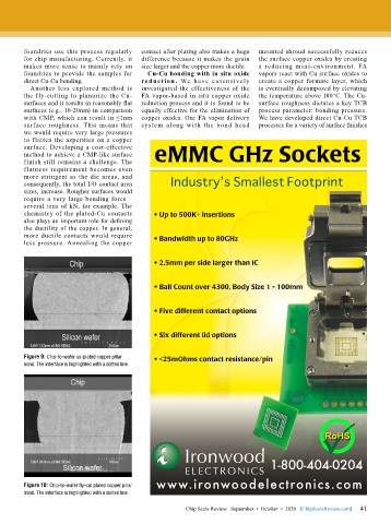
        Figure 9: Chip-to-wafer as-plated copper pillar
        bond. The interface is highlighted with a dotted line.


                                                                                                 P
                                                                                                  RoHS


        Figure 10: Chip-to-wafer fly-cut plated copper pillar
        bond. The interface is highlighted with a dotted line.

                                                                                                             41
                                                         Chip Scale Review   September  •  October  •  2020   [ChipScaleReview.com]  41

