Page 40 - ChipScale_Sep-Oct_2020-digital
P. 40
metal and simultaneously forms a bond. The complexities involved
                                                            during the material preparation make it extremely difficult to
                                                      © 2017 Brewer Science, Inc.
                                                            implement in a production environment [2]. Another approach, also
                                                            proposed by Intel, relies on breaking thin native oxides on In and
                                                            Sn surfaces by applying sufficiently high pressure before reaching
            Creating Safe                                   the melting point in an inert environment. For some processes,
                                                            the temperature is raised close to, but lower than the melting point
                                                            of the solder to promote solid-state diffusion. This method also
            Environments                                    requires a noble metal finish on one of the mating surfaces, and
                                                            additionally requires an inert environment for a reliable bond [3].
                                                              Metal-based interconnects. Metal-metal TCB provides the
                                                            unique advantage of eliminating the solder materials. Consequently,
                                                            the reliance on flux materials to remove oxides can be completely
            Laser Release System                            eliminated. Other than using the noble metal finishes (e.g., Au, Pt,
                                                            etc.), most metals (e.g., Cu, Sn, etc.) would require some method to
            In the laser release system, the device wafer   remove the existing native oxides prior to and during the bonding
            is bonded to a transparent glass carrier using   process. In addition, metal-metal bonding has some very stringent
                                                            requirements for reliable bonding, which include planarity, atomic-
            a bonding material and a release material.      level flatness and removal of native oxide. The TCB process further
            Once processing is completed, the pair is       facilitates the solid-state diffusion. Out of available material
                                                            choices, Cu is of keen interest because it offers excellent material
            separated by exposing the release material      properties and is economically viable. Oxidation prevention on
            with an excimer laser or solid-state laser. Low-  Cu-surfaces, however, is a major challenge. Bajwa, et al. [4], have
                                                            shown that using a noble metal finish (e.g., gold) protects it from
            stress separation coupled with high throughput   oxidation, but this approach adds severe processing complexities.
            make the laser release system suitable for all   Noble metal finish is currently not a standard practice in foundries
                                                            and it will require noble metal finishing on the chips as well as the
            production environments.                        substrates to achieve its purpose.
                                                              More recently, plasma pre-treatments and other in situ oxide
                                                            reduction techniques (e.g., forming gas reduction) have been used
                                                            to reduce and prevent oxidation, but they are more applicable to
                                                            wafer-to-wafer (W2W) processes [6-9]. More often, these methods
                                     Laser                  are employed in controlled environments such as vacuum, N 2 , etc.
                  Transparent
                     Carrier                                Another major hurdle during metal-metal bonding is the roughness
                                           Thin Device Wafer
                                                            of the joining surfaces and planarity of the chip to the target
           Release Layer                  Bonding Material  substrate. Though chemical mechanical planarization (CMP) can
                                                            effectively resolve this issue, it is only applicable to semiconductor
                                                            materials (e.g., Si) and cannot be extended to laminates or PCBs.
                                                            Other techniques, such as fly-cutting of the copper pillars, can be
                                                            potentially useful, but there is very limited data on its applicability.

                                                            Formic acid vapor delivery system
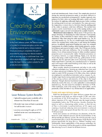
               Laser Release System Benefits:                 K&S has developed an FA vapor delivery system that can
                                                            be integrated with both our chip-to-wafer (C2W) and chip-
                •Highest-throughput system available with a   to-substrate (C2S) TCB machines. The delivery system
                 release time of less than 30 seconds       allows injection of FA vapor directly onto the target surfaces
                                                            immediately before the TCB process, thereby cleaning the
                •Ultraviolet laser does not heat or penetrate   metal as well as eliminating solder oxides, so that the use
                 the bulk bonded structure                  of flux is eliminated. Localized delivery of FA vapors and
                                                            creating a localized reducing mini-environment is achieved
                •Low-stress processing through use of CTE-  through a custom-designed shroud that fits over a standard
                 matched carrier and room temperature       TCB bond head.
                                                              In the next sections we will discuss the chemistry of the FA-
                 separation                                 based tin oxide reduction process and the functionalities of the
                                                            shroud and the gas delivery system. We will also provide a set of
              Compatible with:  308 nm  343 nm  355 nm      experimental data to clarify the performance of the fluxless TCB
                                                                                                  2
                                                            process specifically for large die (i.e., 900mm  bonding case).
                                                            Additionally, future applicability of the process technology for
                                                            Cu-to-Cu interconnect will be discussed as will the experimental
            www.brewerscience.com                           data showing Cu-to-Cu bonds for different devices.


        38   Chip Scale Review   September  •  October  •  2020   [ChipScaleReview.com]
        38

