Page 44 - ChipScale_Sep-Oct_2020-digital
P. 44
Ang, J. Wei, K. C. Leong, “Low-
                                                                                   t e m p e r at u r e C u C u t he r mo -
                                                                                   c o m p r e s s i o n b o n d i ng w i t h
                                                                                   temporary passivation of self-
                                                                                   assembled  monolayer  and  its
                                                                                   bond strength enhancement,”
                                                                                   Microelectronics Rel. 52, no. 2,
                                                                                   pp. 321-324, 2012.
                                                                                 8. K. Tanaka, W-S. Wang, M. Baum,
                                                                                   J. Froemel, H. Hirano, S. Tanaka,
                                                                                   et al., “Investigation of surface
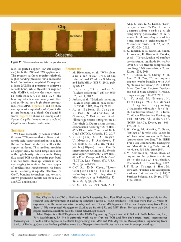
        Figure 11: Chip-to-substrate as-plated copper pillar bond.                 pre-treatment methods for wafer-
                                                                                   level Cu-Cu thermocompression
        (e.g., as-plated copper, fly-cut copper,   References                      bonding,” Micromachines 7, no.
        etc.) for both C2W and C2S applications.   1.  M. Bixenman, et al., “Why clean   12, pp. 234, 2016.
        The rougher surfaces require relatively   a no-clean f lux,” Proc. of the   9.  S. L. Chua, G. Y. Chong, Y. H.
        higher bonding pressure for a successful   International Conf. on Soldering   Lee, C. S. Tan, “Direct copper-
        bond. For instance, as-plated Cu required   and Reliability (ICSR) 2016, pub.   copper wafer bonding with Ar/
        at least 250MPa of pressure to achieve a   by SMTA.                        N 2  plasma activation,” 2015 IEEE
        reliable bond, while fly-cut Cu required   2. Lie, et al., “Approaches for   Inter. Conf. on Electron Devices
        only 80MPa to achieve the same results.   fluxless soldering,” US 6848610   and Solid-State Circuits (EDSSC),
        In both cases, C2W and C2S, the         B2, Feb. 1, 2012.                  Singapore, pp. 134-137, 2015.
        bonding interface was nearly void free   3. Jadhav, et al., “Methods including   10.    Y. A r a i , M . N i m u r a , H .
        and exhibited very high shear strength   fluxless chip attach processes,”   To m o k a g e , “ C u - C u d i r e c t
        (i.e., ≥150MPa). Figures 9 and 10 show   US 7534715 B2, May 19, 2009.      b o n d i n g  t e c h n o log y  u s i n g
        examples of as-plated and fly-cut die   4. A . A . Ba j wa , S . J a ng a m ,   ultrasonic vibration for f lip-
        pillars bonded to a blank Cu-plated Si   S . P a l , N . M a r a t h e , M .   chip interconnection,” 2015 Inter.
        wafer. Figure 11 shows an example of a   Goorsky, T. Fukushima, et al.,     Conf. on Electronics Packaging
        fly-cut Cu pillar bonded to an as-plated   “Heterogeneous integration at   a nd i M A PS A l l A sia C on f.
        Cu pillar on a laminar substrate.       fine pitch (≤10μm) using thermal   (ICEP-IAAC), Kyoto, pp. 468-
                                                compression bonding,” 2017 IEEE    472, 2015.
        Summary                                 67th Electronic Comp. and Tech.   11. W. Yang, M. Akaike, T. Suga,
          We have successfully demonstrated a   Conf. (ECTC), Orlando, FL, 2017.   “Effect of formic acid vapor in
        flux-less TCB process that utilizes in situ   5. S . J a ng a m , A .  A . Ba j wa ,   situ treatment process on Cu low-
        formic acid vapor application to reduce   U. Moge r a , P. A mbhore, T.    temperature bonding,” in IEEE
        the oxide from solder as well as the    Colosimo, R. Chylak, “Fine-        Trans. on Components, Packaging
        copper surfaces. This method provides   pitch  (≤10µm)  direct  Cu- Cu     and Manufacturing Tech., vol. 4,
        an opportunity to bond large area dies   interconnects using in situ formic   no. 6, pp. 951-956, June 2014.
        with high-density interconnects. Using   acid vapor treatment,” 2019 IEEE   12. M. Schmeißer, “Reduction of
        flux-based TCB would require post-bond   69th Elec. Comp. and Tech. Conf.   copper oxide by formic acid an
        flux residuals cleanup, which is very   (ECTC), Las Vegas, NV, USA,        ab-initio study,” Fraunhofer,
        challenging to achieve for these types   2019, pp. 620-627.                Chemnitz U. of Technology, 2012.
        of applications. Furthermore, FA-based   6. C-T. Ko, K-N. Chen, “Low-   13. T. G. A. Youngs, S. Haq, M.
        in situ cleaning is equally effective for   t e m p e r a t u r e b o n d i ng   Bowker, “Formic acid adsorption
        Cu-Cu bonding technology and we have    technology for 3D integration,”    and oxidation on Cu (110),”
        shown promising results for both C2W    Microelectronics Reliability 52,   Surface Science, no. 10, pp. 1775-
        and C2S applications.                   no. 2, 2012, pp. 302-311.          1782, 2008.
                                              7.  C. S. Tan, L. Dau Fatt, X. F.


                       Biographies
                         Bob Chylak is the CTO at Kulicke & Soffa Industries, Inc., Fort Washington, PA. He is responsible for the
                       research and development of packaging solutions across all K&S products.  Bob has more than 30 years of
                       experience in the semiconductor industry and has BS and MS degrees in Electrical Engineering from Penn
                       State U. He completed Management Studies at Stanford U. and MIT Sloan. He has published more than 50
                       papers and holds multiple patents. Email bchylak@kns.com
                         Adeel Bajwa is a Staff Engineer in the R&D Engineering Department at Kulicke & Soffa Industries, Inc.,
                       Fort Washington, PA. He is currently working on fluxless TCB and fine-pitch metal-metal interconnect
          technologies. He holds a BSc degree in Electrical Engineering and MSc and PhD degrees in Microsystems Engineering from
          the U. of Freiburg, Germany. He has published more than 50 papers in scientific journals and conference proceedings.


        42
        42   Chip Scale Review   September  •  October  •  2020   [ChipScaleReview.com]

