Page 46 - ChipScale_Sep-Oct_2020-digital
P. 46

condition to an operating condition. In
                                                                              establishing the acceleration models for
                                                                              lead-free interconnects, their surrounding
                                                                              materials (e.g., solder, molding plastic,
                                                                              ceramic, copper, fiber-reinforced glass
                                                                              epoxy, and silicon), loadings (e.g.,
                                                                              stress, strain, temperature, humidity,
                                                                              current density, and voltage), and failure
                                                                              mechanisms and modes (e.g., overload,
                                                                              fatigue, corrosion, and electromigration)
                                                                              must be considered.
                                                                                Objective of qualification testing.
                                                                              Unlike reliability tests, the objective
                                                                              of qualification tests is “PASS” or
                                                                              “NOT PASS” and the test time is well-
                                                                              defined ahead of time. As soon as there
                                                                              is a failure before the agreed test time,
                                                                              the test will usually stop and failure
                                                                              analysis is performed to find out why the
                                                                              failure occurred. After all the changes,
                                                                              e.g., redesign, a new qualification test
                                                                              will start again. The sample size of
                                                                              qualification tests is usually less than
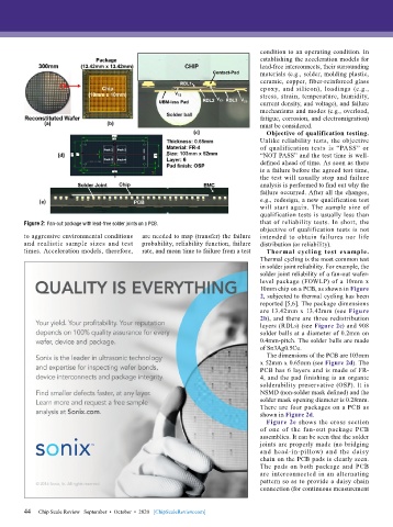
        Figure 2: Fan-out package with lead-free solder joints on a PCB.      that of reliability tests. In short, the
                                                                              objective of qualification tests is not
        to aggressive environmental conditions   are needed to map (transfer) the failure   intended to obtain failures nor life
        and realistic sample sizes and test   probability, reliability function, failure   distribution (or reliability).
        times. Acceleration models, therefore,   rate, and mean time to failure from a test   Thermal cycling test example.
                                                                              Thermal cycling is the most common test
                                                                              in solder joint reliability. For example, the
                                                                              solder joint reliability of a fan-out wafer-
                                                                              level package (FOWLP) of a 10mm x
                                                                              10mm chip on a PCB, as shown in Figure
                                                                              2, subjected to thermal cycling has been
                                                                              reported [5,6]. The package dimensions
                                                                              are 13.42mm x 13.42mm (see Figure
                                                                              2b), and there are three redistribution
                                                                              layers (RDLs) (see Figure 2c) and 908
                                                                              solder balls at a diameter of 0.2mm on
                                                                              0.4mm-pitch. The solder balls are made
                                                                              of Sn3Ag0.5Cu.
                                                                                The dimensions of the PCB are 103mm
                                                                              x 52mm x 0.65mm (see Figure 2d). The
                                                                              PCB has 6 layers and is made of FR-
                                                                              4, and the pad finishing is an organic
                                                                              solderability preservative (OSP). It is
                                                                              NSMD (non-solder mask defined) and the
                                                                              solder mask opening diameter is 0.28mm.
                                                                              There are four packages on a PCB as
                                                                              shown in Figure 2d.
                                                                                Figure 2e shows the cross section
                                                                              of one of the fan-out package PCB
                                                                              assemblies. It can be seen that the solder
                                                                              joints are properly made (no bridging
                                                                              and head-in-pillow) and the daisy
                                                                              chain on the PCB pads is clearly seen.
                                                                              The pads on both package and PCB
                                                                              are interconnected in an alternating
                                                                              pattern so as to provide a daisy chain
                                                                              connection (for continuous measurement


        44
        44   Chip Scale Review   September  •  October  •  2020   [ChipScaleReview.com]
   41   42   43   44   45   46   47   48   49   50   51