Page 37 - ChipScale_Sep-Oct_2020-digital
P. 37
Summary
                                                                                Heterogeneous packaging is going to
                                                                              be the main driver for today’s and future
                                                                              semiconductor packaging in a variety
                                                                              of applications from system in package
                                                                              (SiP) to chiplet packaging. The main
                                                                              process challenge for these multi-chip
                                                                              expensive packages remains how to keep
                                                                              the package cost as low as possible so
                                                                              we can reference Moore’s Law as being
                                                                              economically valid, even 50-plus years
                                                                              after the invention of integrated circuits.
                                                                              Final package inspection is the last
                                                                              process step to determine heterogeneous
                                                                              package/product yield. Therefore, having
                                                                              the  most  capable  solution  for  final
                                                                              package 2D/3D inspection is inevitable in
                                                                              order to enable heterogenous packaging
                                                                              and drive the industry forward.
                                                                                Our key vision capabilities such as
                                                                              large field of view (FOV), stitching, and
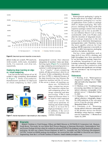
        Figure 6: Deep-learning second-inspection process results.            high throughput, have been specialized

        defect modes are scratch, FM (particle),   management system. Our coherent   by our heterogenous package inspection.
        mold scratch, mold crack, incomplete   integration of machine vision and deep-  In addition, integration of our deep-
        mold, Cu exposed, and chip-out,    learning engine (Figure 5), is considered   learning technology and machine vision
        respectively.                      as edge computing (processing) prior to a   into one process has resulted in yield
                                           customer’s yield management process.  improvement and significant cost savings
        Deploying deep learning on edge      In  a “regular”  cloud-computing   for our customers: top heterogeneous
        vs. cloud computing                system, all data processing is done by an   chip makers.
          Last, but not the least feature of our AI   AI server. In this configuration, the units
        system is edge computing, demonstrated   per hour (UPH) is impacted because of   References
        in  Figure 7. Some semiconductor   the data transferring time between the   1.  P. Wesling, et al., “Heterogeneous
        manufacturers perform AI deployed   inspection machine and the AI server.   integration roadmap,” Ch. 8: Single-
        on cloud computing by their yield   If the server is down, all machines are   chip and multi-chip integration,” IEEE
                                                      down too. INTEKPLUS         2019 Edition.
                                                      edge computing means      2.  S. Chitchian, et al., “Combined image
                                                      the inspection engine has   processing algorithms for improved
                                                      self-computing power for    optical coherence tomography of the
                                                      image capturing and data    prostate nerves,” J. Biomedical Optics
                                                      processing.  UPH  is not    15, 2010.
                                                      impacted because there is   3.  S. Chitchian, et al., “Segmentation of
                                                      no need to send inspection   optical coherence tomography images
                                                      images to a server. The     for differentiation of the cavernous
                                                      cloud server performs AI    nerves from the prostate gland,” J.
                                                      learning and model training   Biomedical Optics 14, 2009.
                                                      so there is no need for a   4.  S. Chitchian, et al., “Denoising
                                                      high-performance server.    during optical coherence tomography
                                                      In addition, if the server   of the prostate nerves via wavelet
                                                      is down, all machines can   shrinkage using dual-tree complex
                                                      continue running.           wavelet transform,” J. Biomedical
        Figure 7: Deep learning deployed on edge computing vs. cloud computing.   Optics 14, 2009.


                       Biography
                         Shahab Chitchian is Chief Strategy Officer and R&D Director at INTEKPLUS Corporation Ltd., Daejeon,
                       South Korea. Previously, he was Senior Staff Process Engineer at Samsung Electronics, Semiconductor Test
                       and System Package division where he worked on advanced FOWLP development and high-bandwidth memory
                       packaging. He also was a Senior Process Engineer at Intel Co., Assembly and Test Technology Development
                       (ATTD), worked on EMIB package development. He received his MSc and PhD in Electrical and Optical
                       Engineering, from the U. of North Carolina at Charlotte. Email shahab@intekplus.com


                                                                                                             35
                                                         Chip Scale Review   September  •  October  •  2020   [ChipScaleReview.com]  35

