Page 32 - ChipScale_Sep-Oct_2020-digital
P. 32
the industry has focused its   and several months’ worth of lead time for a
                                                       efforts on the flip-chip chip-  new substrate design (Figure 11).
                                                       scale package (FCCSP)
                                                       style of AiP, where patch
                                                       antennas are on the top
                                                       surface of the substrate
                                                       with dipole antennas (Yagi-
                                                       Uda antennas) around the
                                                       peripherals. However, the
                                                       lossy nature of the organic
                                                       substrate and large form
                                                       factor can be problematic for
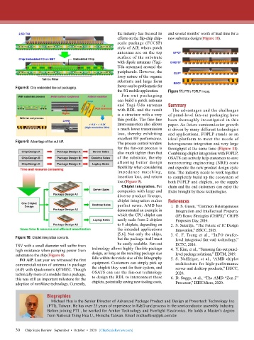
        Figure 8: Chip embedded fan-out packaging.
                                                       the 5G mobile application.  Figure 11: PTI’s FOPLP lineup.
                                                         Fa n- out pa ck ag i ng
                                                       can build a patch antenna
                                                       and Yagi-Uda antenna   Summary
                                                       with RDL and the result   The advantages and the challenges
                                                       is a structure with a very   of panel-level fan-out packaging have
                                                       thin profile. The fine-line   been thoroughly investigated in this
                                                       interconnection also allows   paper. As future semiconductor growth
                                                       a much lower transmission   is driven by many different technologies
                                                       loss, thereby exhibiting   and applications, FOPLP stands as an
                                                       excellent RF performance.   ideal platform to meet the needs of
        Figure 9: Advantage of fan-out AiP.            The process control window   heterogeneous integration and very large
                                                       for the fan-out process is   throughput at the same time (Figure 11).
                                                       also much tighter than that   Combining chiplet integration with FOPLP,
                                                       of the substrate, thereby   OSATS can actively help customers to save
                                                       allowing better design   nonrecurring engineering (NRE) costs
                                                       flexibility when considering   and expedite the new product design cycle
                                                       impedance matching,    time. The industry needs to work together
                                                       insertion loss, and return   to completely build up the ecosystem of
                                                       loss (Figure 9).       both FOPLP and chiplets, so the supply
                                                         Chiplet integration. For   chain and the end customers can enjoy the
                                                       companies with large and   fruits brought by these technologies.
                                                       diverse product lineups,
                                                       chiplet integration makes   References
                                                       perfect sense. AMD has   1.  D. S. Green, “Common Heterogeneous
                                                       demonstrated an example in   Integration and Intellectual Property
                                                       which the CPU chiplet can   (IP) Reuse Strategies (CHIPS),” CHIPS
                                                       easily scale from 2 chiplets   Proposers Day, 2016.
                                                       to 8 chiplets, depending on   2.  S. Sutardja, “The Future of IC Design
                                                       the intended applications   Innovation,” ISSCC, 2015.
                                                       [5,6]. Not only the chips,   3.  C. F. Tseng et al., “InFO (wafer-
        Figure 10: Chiplet integration scenario.       but the package itself must   level integrated fan-out) technology,”
        TSV with a small diameter will suffer from     be easily scalable. Fan-out   ECTC, 2016.
        high resistance when pumping power from   technology allows highly flexible package   4.  Y. Kim, et al., “Samsung fan-out panel-
        substrate to the chip (Figure 8).  design, as long as the resulting package size   level package solutions,” EDTM, 2019.
          FO AiP. Last year we witnessed the first   falls within the reticle size of the lithography   5.  S. Naffziger, et al., “AMD chiplet
        commercialization of antenna in package   equipment. Customers can simply pick up   architecture for high-performance
        (AiP) with Qualcomm’s QTM052. Though   the chiplets they want for their system, and   server and desktop products,” ISSCC,
        technically more of a module than a package,   OSATS can use the fan-out technology   2020.
        this was still an important milestone for the   to design the RDL to interconnect these   6.  D. Suggs, et al., “The AMD “Zen 2”
        adoption of mmWave technology. Currently,   chiplets, potentially saving new tooling costs,   Processor,” IEEE Micro, 2020.

                       Biographies
                         Michael Hsu is the Senior Director of Advanced Package Product and Design at Powertech Technology Inc
                       (PTI), Taiwan. He has over 25 years of experience in R&D and process in the semiconductor assembly industry.
                       Before joining PTI , he worked for Amkor Technology and Everlight Electronics. He holds a Master’s degree
                       from National Tsing Hua U., Hsinchu Taiwan. Email michaelhsu@pti.com.tw


        30
        30   Chip Scale Review   September  •  October  •  2020   [ChipScaleReview.com]

