Page 30 - ChipScale_Sep-Oct_2020-digital
P. 30
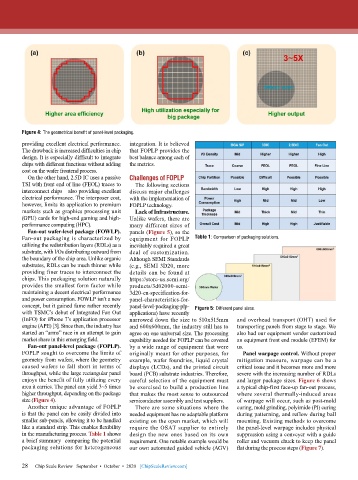
Figure 4: The geometrical benefit of panel-level packaging.
        providing excellent electrical performance.   integration. It is believed
        The drawback is increased difficulties in chip   that FOPLP provides the
        design. It is especially difficult to integrate   best balance among each of
        chips with different functions without adding   the metrics.
        cost on the wafer frontend process.
          On the other hand, 2.5D IC uses a passive   Challenges of FOPLP
        TSI with front end of line (FEOL) traces to   The following sections
        interconnect chips—also providing excellent   discuss major challenges
        electrical performance. The interposer cost,   with the implementation of
        however, limits its application to premium   FOPLP technology.
        markets such as graphics processing unit   Lack of Infrastructure.
        (GPU) cards for high-end gaming and high-  Unlike wafers, there are
        performance computing (HPC).       many different sizes of
          Fan-out wafer-level package (FOWLP).   panels (Figure 5), so the
        Fan-out packaging is characterized by   equipment for FOPLP   Table 1: Comparison of packaging solutions.
        utilizing the redistribution layers (RDLs) as a   inevitably required a great
        substrate, with I/Os distributing outward from   deal of customization.
        the boundary of the chip area. Unlike organic   Although SEMI Standards
        substrates, RDLs can be much thinner while   (e.g., SEMI 3D20, more
        providing finer traces to interconnect the   details can be found at
        chips. This packaging solution naturally   https://store-us.semi.org/
        provides the smallest form factor while   products/3d02000-semi-
        maintaining a decent electrical performance   3d20-en-specification-for-
        and power consumption. FOWLP isn’t a new   panel-characteristics-for-
        concept, but it gained fame rather recently   panel-level-packaging-plp-  Figure 5: Different panel sizes.
        with TSMC’s debut of Integrated Fan Out   applications) have recently
        (InFO) for iPhone 7’s application processor   narrowed down the size to 510x515mm   and overhead transport (OHT) used for
        engine (APE) [3]. Since then, the industry has   and 600x600mm, the industry still has to   transporting panels from stage to stage. We
        started an “arms” race in an attempt to gain   agree on one universal size. The processing   also had our equipment vendor customized
        market share in this emerging field.   capability needed for FOPLP can be covered   an equipment front end module (EFEM) for
          Fan-out panel-level package (FOPLP).   by a wide range of equipment that were   us.
        FOPLP sought to overcome the limits of   originally meant for other purposes, for   Panel warpage control. Without proper
        geometry from wafers, where the geometry   example, wafer foundries, liquid crystal   mitigation measure, warpage can be a
        caused wafers to fall short in terms of   displays (LCDs), and the printed circuit   critical issue and it becomes more and more
        throughput, while the large rectangular panel   board (PCB) substrate industries. Therefore,   severe with the increasing number of RDLs
        enjoys the benefit of fully utilizing every   careful selection of the equipment must   and larger package sizes. Figure 6 shows
        area it carries. The panel can yield 3~5 times   be exercised to build a production line   a typical chip-first face-up fan-out process,
        higher throughput, depending on the package   that makes the most sense to outsourced   where several thermally-induced areas
        size (Figure 4).                   semiconductor assembly and test suppliers.  of warpage will occur, such as post-mold
          Another unique advantage of FOPLP   There are some situations where the   curing, mold grinding, polyimide (PI) curing
        is that the panel can be easily divided into   needed equipment has no adaptable platform   during patterning, and reflow during ball
        smaller sub-panels, allowing it to be handled   existing on the open market, which will   mounting. Existing methods to overcome
        like a standard strip. This enables flexibility   require the OSAT supplier to entirely   the panel-level warpage includes physical
        in the manufacturing process. Table 1 shows   design the new ones based on its own   suppression using a conveyer with a guide
        a brief summary  comparing the potential   requirement. One notable example would be   roller and vacuum chuck to keep the panel
        packaging solutions for heterogeneous   our own automated guided vehicle (AGV)   flat during the process steps (Figure 7).


        28   Chip Scale Review   September  •  October  •  2020   [ChipScaleReview.com]
        28

