Page 29 - ChipScale_Sep-Oct_2020-digital
P. 29
FOPLP as a solution for heterogeneous integration


        By Michael Hsu  [Powertech Technology Inc.]
        I     t’s been several decades since the   of SoC are becoming prohibitive [1,2]   either wire bonded or flip-chip bonded to


              invention of integrated circuits
                                           are needed to amortize the cost quickly. The
                                                                              to suffer from parasitic capacitance or
              (ICs)—but the proliferation of them   (Figure 1) because large demand quantities   the substrate. The wire bonded chips tend
        has reshaped our way of life. Though Moore’s                          inductance at higher frequencies, and such
        Law, which observed this proliferation, is
        now facing difficulty moving forward, we did
        not come this far to see it end prematurely,
        so the industry has been working and
        collaborating for its continuation.
          There are two trends in the industry that
        have been seeking to extend Moore’s Law:
        1) “More than Moore” led by foundries,
        and 2) “More than Moore” spearheaded by
        outsourced semiconductor assembly and test
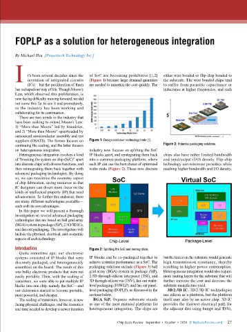
        suppliers (OSATS). The former focuses on   Figure 1: Design cost over technology node [1].
        continuing the scaling, and the latter focuses                        Figure 3: Potential packaging solutions.
        on  heterogeneous integration.     industry now focuses on splitting the SoC
          Heterogeneous integration involves a kind   IP blocks apart, and reintegrating them back   chips also have rather limited bandwidth
        of “breaking the system on chip (SoC)” apart   into a common packaging platform, where   and input/output (I/O) density. Flip-chip
        into discrete chips with diverse functions, and   each IP can use the best choice of optimized   technology can minimize parasitics while
        then reintegrating them back together with   wafer node (Figure 2). These now discrete   reaching higher bandwidth and I/O density,
        advanced packaging technologies. By doing
        so, we can maximize the economy aspect
        of chip fabrication, saving resources so that
        IC designers can divert more focus on the
        kinds of intellectual property (IP) that need
        advancement. To further this endeavor, there
        are many different technologies available—
        each with its own advantages.
          In this paper we will present a thorough
        investigation on several advanced packaging
        technologies that are based on ball grid array
        (BGA) system in package (SiP), 2.5D/3D ICs,
        and fan-out packaging. The investigation will
        include the physical, electrical, and economic
        aspects of each technology.
        Introduction                       Figure 2: Splitting the SoC and reintegration.
          Quite sometime ago, our electronic
        systems consisted of IP blocks that were   IP blocks can be co-packaged together to   but the traces on the substrate would generate
        discretely packaged, and heterogeneously   achieve a similar performance as a SoC. The   high transmission resistance, thereby
        assembled on the board. The result of this   packaging solutions include (Figure 3) ball   resulting in higher power consumption.
        was bulky electronic products that were not   grid array (BGA) system in package (SiP),   Heterogeneous integration would also require
        easily portable. Then, with the scaling of   2.5D through-silicon interposer (TSI), and   more routing layers for the substrate that will
        transistors, we were able to put multiple IP   3D through-silicon via (TSV), fan-out wafer-  further increase the cost and decrease the
        blocks into one chip, namely the SoC—and   level packaging (FOWLP), and fan-out panel-  substrate manufacture yield.
        our electronics started to become portable,   level packaging (FOPLP), as discussed in the   3D/2.5D IC. 3D/2.5D IC technologies
        more powerful, and cheaper.        sections below.                    use silicon as a platform, but the platform
          The scaling of transistors, however, is now   BGA SiP. Organic substrate stands   itself may also be an active chip. 3D IC
        facing physical challenges, and the resources   as one of the most matured platforms for   provides the shortest electrical path for
        and time needed to develop a newer iteration   heterogeneous integration. The chips are   the adjacent dies using bumps and TSVs,


                                                                                                             27
                                                         Chip Scale Review   September  •  October  •  2020   [ChipScaleReview.com]  27

