Page 31 - ChipScale_Sep-Oct_2020-digital
P. 31
last process also makes it much easier to
                                                                              attach passive devices of varying sizes.  We
                                                                              have a standing solution called CLIP  (Chip
                                                                                                         ®
                                                                              Last Integration Package).
                                                                                For heterogeneous integration, the chip-
                                                                              last approach is an ideal platform whereby
                                                                              many different chips and passives can
                                                                              be easily integrated in a common RDL
                                                                              substrate, and is one in which the fine-
                                                                              line RDL allows them to be put in close
                                                                              proximity. It is also a good alternative to the
                                                                              2.5D IC, which requires a very expensive
                                                                              Si interposer with TSV. For example, for
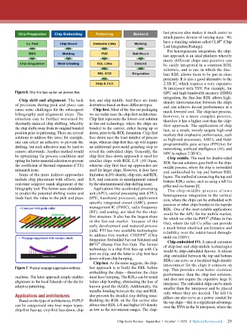
        Figure 6: Chip-first face-up fan-out process flow.                    GPU and high-bandwidth memory (HBM)
                                                                              integration, the fine-line RDL allows high-
          Chip shift and alignment. The lack   last, and chip middle. And there are many   density interconnection between the chips
        of precision during pick and place can   derivatives based on these different types.  and can achieve decent performance at a
        cause some challenges for the subsequent   Chip first. Most of the fan-out packaging   much lowered cost. The chip-last process,
        lithography and alignment steps. The   we see today uses the chip-first architecture.   however, is a more complex process,
        situation can be further worsened by   Chip first represents the lowest cost solution   therefore it has a higher cost than the chip-
        thermally-induced chip shifting, whereby   in fan-out technology, where the chips are   first approach. The application of chip
        the chip shifts away from its original bonded   bonded to the carrier, either facing up or   last, as a result, mostly targets high-end
        position prior to patterning. There are several   down, prior to the RDL formation. Chip-first   markets that emphasize performance, such
        solutions to address this issue; for example,   face-down uses the least number of process   as high-end processors, ASICs, and field-
        one can select an adhesive to prevent the   steps, whereas chip-first face-up will require   programmable gate arrays (FPGAs) for
        shifting, but such adhesives may be hard to   an additional post-mold grinding step to   networking, artificial intelligence (AI), and
        remove afterwards. Another method would   reveal the embedded chips. Generally, the   HPC to replace 2.5D ICs.
        be optimizing the process conditions and   chip-first face-down approach is used for   Chip middle. The need for double-sided
        opting for better material selection to prevent   smaller chips with RDL L/S ≥10/10µm,   RDL fan-out solutions gave birth to the chip-
        the coefficient of thermal expansion (CTE)   whereas chip-first face-up approaches are   middle process, where the chip is embedded
        mismatch issue.                    used for larger chips. However, it does have   and sandwiched by top and bottom RDL
          Some of the more indirect approaches   limitation in I/O density, chip size, and RDL   layers. The method of connecting the top and
        include chip placement with offsets, and   L/S, and concerns in misalignment caused   bottom RDLs varies, such as using a tall Cu
        real-time adaptive mask alignment of the   by the aforementioned chip shifting issue.  pillar and via frames [4].
        lithography tool. The former uses simulation   Applications like accelerated processing   The chip-middle process allows
        to predict the potential shifting vector and   unit (APU), central processing unit (CPU),   heterogeneous integration in the vertical
        feeds back the value to the pick and place   GPU, baseband processor, application   axis, where the chips can be embedded with
                                           specific integrated circuit (ASIC), power   passives or other chips bonded to the topside
                                           management IC (PMIC), radio frequency   RDL. One of the most notable applications
                                           (RF), and analog, are ideal for the chip-  would be the APU for the mobile market,
                                           first structure. It also has the largest share   for which we offer the PiFO  (Pillars in Fan
                                                                                                   ®
                                           in the fan-out market  because of the   Out), where the tall Cu pillar can provide
                                           early development and matured process   a much better electrical performance and
                                           yield. PTI has two available technologies   reliability over the solder-based through-
                                                                      ®
                                           to address this market: CHIEFS  (Chip   mold via (TMV).
                                           Integration Embedded Fan out Solution) and   Chip-embedded FO. A natural extension
                                              2
                                                ®
                                           BF O  (Bump Free Fan Out). The former   of chip-last and chip-middle technologies
                                           technology is a chip first face up with Cu   would be chip-embedded fan-out. A silicon
                                           post on chip, and the latter is chip first face   chip embedded between the top and bottom
                                           down without chip bumping.         RDLs can serve as a localized high-density
                                             Chip last. As the name suggests, the chip-  interconnect for the chips it connects on
        Figure 7: Physical warpage suppression methods.  last approach is to build the RDL before   top. This provides even better electrical
                                           embedding the chips—therefore the chips   performance than the chip-last solution,
        machine. The latter approach simply enables   must have bumping. The RDLs can be tested   and does not require the expensive large Si
        alignment to the local fiducials of the die for   before chip bonding, eliminating the loss of   interposer. The embedded chips can be much
        adaptive patterning.               known good die (KGD). Additionally, the   smaller than the interposer and be placed
                                           metallic bonding between the chip and RDL   only where they are needed. The tall Cu
        Applications and architectures     also prevents the dreaded chip shifting issue.   pillars can also serve as a power conduit for
          Based on the type of architectures, FOPLP   Building the RDL on the flat carrier also   the top chips—this is a significant advantage
        can be categorized into four major types:   allows finer RDL L/S and higher I/O density   over the TSVs in the Si interposer, where the
        chip-first face-up, chip-first face-down, chip   as low as the sub-micron ranges. The chip-

                                                                                                             29
                                                         Chip Scale Review   September  •  October  •  2020   [ChipScaleReview.com]  29

