Page 26 - ChipScale_Sep-Oct_2020-digital
P. 26
top of an organic substrate. Therefore,   to achieve the best performance. The   process by offering passive and active
        the board-level stress can be mitigated   resultant 3D-IC structure will continue   embedding capability along with their
        by t h e s u b s t r a t e , w h ich c a n b e   to follow Moore’s Law. Besides SRAM,   substrate business. Although OSATS
        considered a stress buffer.        there are many other chiplets with   seem to be in a difficult position facing
          E me r g i n g a pp r o ac h : 3 D - I C   different functions at various nodes   competition from both the foundries
        integration.  Besides package-level   that can be mixed and matched by   and substrate suppliers, they are also
        integration,  the  3D-IC  integration   interconnecting them together like the   pushing the development of more cost-
        ap proa ch is b ei ng a dvo cat e d i n   SRAM example given above. Another   effective packaging technology to
        order to achieve the next level of   way to further improve the economics   cope with the emerging but massive
        integration with direct chip-to-chip   is to reuse the intellectual property (IP)   requirements of edge and IoT devices
        interconnection without any external   from not only in-house, but also from   required by the AI world.
        interposer or RDL routing (Figure   multiple third-party chiplets. However,
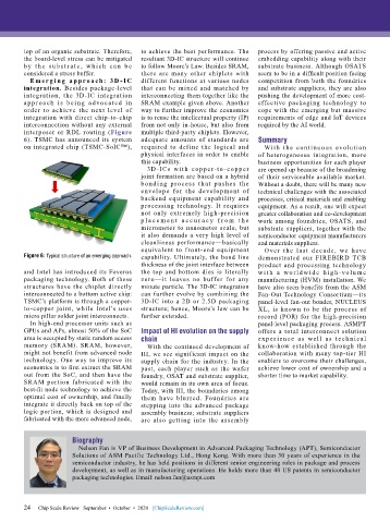
        6). TSMC has announced its system   adequate amounts of standards are   Summary
        on integrated chip (TSMC-SoIC™),   required to define the logical and   With the  conti nuous  evolution
                                           physical interfaces in order to enable   of heterogeneous integration, more
                                           this capability.                   business opportunities for each player
                                             3D -ICs w it h copper-to - copper   are opened up because of the broadening
                                           joint formation are based on a hybrid   of their serviceable available market.
                                           bonding process that pushes the    Without a doubt, there will be many new
                                           envelope for the development of    technical challenges with the associated
                                           backend equipment capability and   processes, critical materials and enabling
                                           processing technology. It requires   equipment. As a result, one will expect
                                           not  only  extremely  high-precision   greater collaboration and co-development
                                           p l a c e m e n t a c c u r a c y f r o m t h e   work among foundries, OSATS, and
                                           micrometer to nanometer scale, but   substrate suppliers, together with the
                                           it also demands a very high level of   semiconductor equipment manufacturers
                                           cleanliness performance—basically   and materials suppliers.
                                           equivalent to front-end equipment    Over the last decade, we have
        Figure 6: Typical structure of an emerging approach.  capability. Ultimately, the bond line   demonstrated our FIREBIRD TCB
                                           thickness of the joint interface between   product and processing technology
        and Intel has introduced its Foveros   the top and bottom dies is literally   w i t h a wo r l d w i d e  h i g h -vol u m e
        packaging technology. Both of these   zero —it leaves no buffer for any   manufacturing (HVM) installation. We
        structures have the chiplet directly   minute particle. The 3D-IC integration   have also seen benefits from the ASM
        interconnected to a bottom active chip:   can further evolve by combining the   Fan-Out Technology Consortium—its
        TSMC’s platform is through a copper-  3D-IC into a 2D or 2.5D packaging   panel-level fan-out bonder, NUCLEUS
        to-copper joint, while Intel’s uses   structure; hence, Moore’s law can be   XL, is known to be the process of
        micro pillar solder joint interconnects.  further extended.           record (POR) for the high-precision
          In high-end processor units such as                                 panel-level packaging process. ASMPT
        GPUs and APs, almost 50% of the SoC   Impact of HI evolution on the supply   offers  a  total  interconnect  solution
        area is occupied by static random access   chain                      exp e r ie nce a s wel l a s t e ch n ical
        memory (SRAM). SRAM, however,        With the continued development of   know-how established through the
        might not benefit from advanced node   HI, we see significant impact on the   collaboration with many top-tier HI
        technology. One way to improve its   supply chain for the industry. In the   enablers to overcome their challenges,
        economics is to first extract the SRAM   past,  each  player  such  as  the  wafer   achieve lower cost of ownership and a
        out from the SoC, and then have the   foundry, OSAT and substrate supplier,   shorter time to market capability.
        SRAM  portion  fabricated  with  the   would remain in its own area of focus.
        best-fit node technology to achieve the   Today, with HI, the boundaries among
        optimal cost of ownership, and finally   them have blurred. Foundries are
        integrate it directly back on top of the   stepping into the advanced package
        logic portion, which is designed and   assembly business; substrate suppliers
        fabricated with the more advanced node,   are also getting into the assembly


                       Biography
                         Nelson Fan is VP of Business Development in Advanced Packaging Technology (APT), Semiconductor
                       Solutions of ASM Pacific Technology Ltd., Hong Kong. With more than 30 years of experience in the
                       semiconductor industry, he has held positions in different senior engineering roles in package and process
                       development, as well as in manufacturing operations. He holds more than 40 US patents in semiconductor
                       packaging technologies. Email: nelson.fan@asmpt.com


        24
        24   Chip Scale Review   September  •  October  •  2020   [ChipScaleReview.com]

