Page 25 - ChipScale_Sep-Oct_2020-digital
P. 25
bridge is only around 6mm x 6mm! There
                                                                              are two important assembly processes
                                                                              involved in making an EMIB. First, in the
                                                                              panel format, single or multiple bridges
                                                                              are embedded into a semi-finished high-
                                                                              density build-up organic substrate with
                                                                              a very high-precision die attach tool.
                                                                              It is then followed by a high-density
                                                                              and fine line and space electrochemical
                                                                              metal deposition (ECD) process for the
                                                                              RDL formation. Moving forward it is
                                                                              foreseeable that when the geometry of chip
                                                                              I/O bump pitch features shrink further, the
                                                                              requirement on bridge placement accuracy
                                                                              will become more stringent.
                                                                                A l t ho u g h E M I B i s i d e a l  f o r
                                                                              integ rating multiple components
                                                                              without the scaling limitations found
                                                                                         ®
                                                                              with CoWoS , there is also concern in
                                                                              deploying this technology. The chip
                                                                              layout needs to align with the package
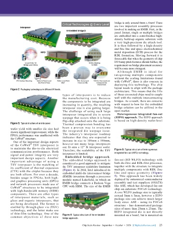
        Figure 2: Packaging technologies in different HI levels.
                                                                              architecture. This means that the I/Os
                                           types of inter posers is to reduce   of those connected chips need to couple
                                           the manufact uring cost. Because   well with the multiple interconnecting
                                           the components to be integrated are   bridges. As a result, there are concerns
                                           increasing in quantity, the resulting   with respect to how far the embedded
                                           interposer size is also getting larger.   bridge solution can be utilized in the
                                           The challenge of using such large   open market.
                                           interposer integrated die is severe   Heterogeneous integrated fan-out
                                           warpage that occurs when it is being   (HIFO) approach. The HIFO approach
                                           flip-chip attached onto the substrate.   is based on high-density wafer-level
        Figure 3: Typical structure of an interposer.  Thermal compression bonding has

        wafer yield with smaller die size had   been a proven way to ove rcome
        shown significant improvement, while the   the integrated die war page issue.
        FPGA performance was unaffected with   The industry’s interposer roadmap
                 ®
        the CoWoS  structure.              indicates that they are expected to
          One of the important design aspects   increase in size to 100mm x 100mm,
        of the CoWoS  TSV inter poser is   however not many large interposers
                      ®
        to maintain the die-to-die electrical   can fit onto a 12” Si interposer wafer.   Figure 5: Typical structure of heterogeneous
        communication performance. Both    Therefore, the scalability of the TSV   integrated fan-out (HIFO) technology.
        signal and power integrity are very   interposer is limited.
        important design aspects. Another    Emb e d de d br i d ge a ppr o ach.   fan-out (HD WLFO) technology with
        i mp or t a nt a dva nt age of u si ng  a   The embedded bridge approach is   both die-first and RDL-first processes,
        TSV interposer is the matching of   considered a good approach to mitigate   together with the structure to integrate
        its coefficient of thermal expansion   the TSV interposer scalability limitation    multiple components with RDL fine
        (CTE) with the chiplet because they   (Figure 4). In 2014, Intel introduced its   line and space geometr y (Figure
        are both silicon. For over a decade,   embedded multi-die interconnect bridge   5).  This  approach  has  been  widely
        besides usage in FPGAs, both high-  (EMIB) invention through a processor   deployed by outsourced semiconductor
        end graphics processing units (GPUs)   module named Lakefield, in which an   assembly and test suppliers (OSATS)
        and network processors made use of   EMIB bridge connects a Radeon Vega   like ASE, which has developed fan-out
               ®
        CoWoS  structures to be integrated   CPU with HBM. The size of the EMIB   chip-on-substrate FOCoS technology.
        with high-bandwidth memory (HBM)                                      A core WLFO package size is typically
        components. There are other types                                     around 5mm x 5mm, however a HIFO
        of i nter poser mater ials, such as                                   package size can achieve much larger
        glass and organic interposers, that                                   body  sizes.  ASE –  using  its  FOCoS
        are being developed.  The  former is                                  structure – has demonstrated package
        enabled by through-glass via (TGV)                                    sizes of more than 25mm x 25mm. The
        technology, and the latter make use                                   HIFO integrated die is not directly
        of thin-film technology. One of the   Figure 4: Typical structure of the embedded   mounted on a board, but is mounted on
        com mon objectives of  these  new   bridge approach.

                                                                                                             23
                                                         Chip Scale Review   September  •  October  •  2020   [ChipScaleReview.com]  23

