Page 23 - ChipScale_Sep-Oct_2020-digital
P. 23
Enabling artificial intelligence with heterogeneous


        integration


        By Nelson Fan  [ASM Pacific Technology Ltd.]
        W            e are at the dawn of the


                     artificial intelligence
                     (AI) era! It will not
        be long before highly-intelligent cars
        enabled by AI will be cruising on our
        highways. Imagine that our future AI-
        enabled homes will automatically cool
        down to the optimal temperature just
        before we arrive home after a hard day’s
        work, and  dinner is prepared and ready
        to serve. At a large scale, cities built
        with embedded AI will be operating
        efficiently with tremendous amounts
        of devices and robots con nected
        through 5G infrastructure with enough
        bandwidth for data management and
 Volta Series Probe Head  transfer. High-performance computing
        (HPC) devices – one of the essential
         Wafer Level Testing From 200µ  elements required for both end-terminals
        and edge computing – are needed for
        analyzing large amounts of data coming
        from massive numbers of (50B units
        by 2025) Internet of Everything (IoT)
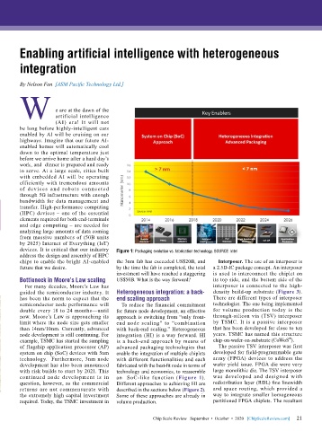
        devices. It is critical that our industry   Figure 1: Packaging evolution vs. fabrication technology. SOURCE: Intel
 Increased Throughput, Reduced Test Time  address the design and assembly of HPC   the 3nm fab has exceeded US$20B, and   Interposer. The use of an interposer is
        chips to enable the bright AI-enabled
        future that we desire.             by the time the fab is completed, the total   a 2.5D-IC package concept. An interposer
 Smiths Interconnect’s Volta Series Probe Head provides improved   investment will have reached a staggering   is used to interconnect the chiplet on
 efficiency in high reliability WLP, WLCSP and KGD testing.  Bottleneck in Moore’s Law scaling  US$50B. What is the way forward?  its top side, and the bottom side of the
          For many decades, Moore’s Law has                                   interposer is connected to the high-
        guided the semiconductor industry. It   Heterogeneous integration: a back-  density build-up substrate (Figure 3).
 ■ Extremely short signal path (≤3.80mm) enables low and stable contact  has been the norm to expect that the   end scaling approach   There are different types of interposer
 resistance, high current carrying capacity and longer life cycle  semiconductor node performance will   To reduce the financial commitment   technologies. The one being implemented
        double every 18 to 24 months—until   for future node development, an effective   for volume production today is the
 ■ Enhanced planarity allows increased site to site test parallelism  now. Moore’s Law is approaching its   approach is switching from “only front-  through-silicon via (TSV) interposer
        limit where the node size gets smaller   end node scaling” to “combination   by TSMC. It is a passive interposer
 ■ Reduced test set-up time, simple maintenance and field  than 14nm/10nm. Currently, advanced   with back-end scaling.” Heterogeneous   that has been developed for close to ten
                                                                              years. TSMC has named this structure
        node development is still continuing. For
 replacement ensure lower cost of ownership  example, TSMC has started the sampling   integration (HI) is a way forward. HI   chip-on-wafer-on-substrate (CoWoS ).
                                                                                                          ®
                                           is a back-end approach by means of
        of flagship application processor (AP)   advanced packaging technologies that   The passive TSV interposer was first
 ■ Allows sorted die test of all sites simultaneously  system on chip (SoC) devices with 5nm   enable the integration of multiple chiplets   developed for field-programmable gate
 resulting in increased test yields in a shorter time  technology.  Furthermore, 3nm node   with different functionalities and each   array (FPGA) devices to address the
        development has also been announced   fabricated with the best-fit node in terms of   wafer yield issue. FPGA die were very
        with risk builds to start by 2021. This   technology and economics, to reassemble   large monolithic die. The TSV interposer
        continued node development is in   an  SoC-like function (Figure 1).   was developed and designed with
        question, however, as the commercial   Different approaches to achieving HI are   redistribution layer (RDL) fine linewidth
 Visit us at IWLPC Virtual Event October 13th-14th 2020  returns are not commensurate with   described in the sections below (Figure 2).   and space routing, which provided a
        the extremely high capital investment   Some of these approaches are already in    way to integrate smaller homogeneous
        required. Today, the TSMC investment in   volume production.          partitioned FPGA chiplets. The resultant

 smithsinterconnect.com
                                                                                                             21
                                                         Chip Scale Review   September  •  October  •  2020   [ChipScaleReview.com]  21

