Page 19 - Chip Scale Review_November-December_2023-digital
P. 19
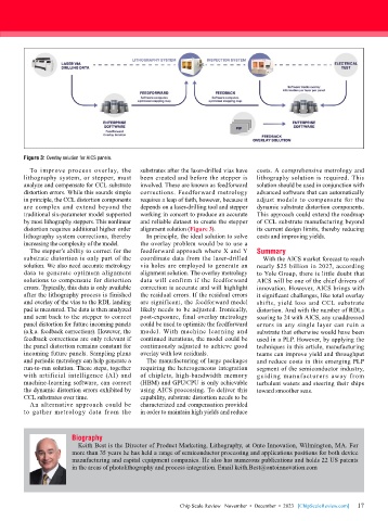
Figure 3: Overlay solution for AICS panels.
          To improve process overlay, the   substrates after the laser-drilled vias have   costs. A comprehensive metrology and
        lithography system, or stepper, must   been created and before the stepper is   lithography solution is required. This
        analyze and compensate for CCL substrate   involved. These are known as feedforward   solution should be used in conjunction with
        distortion errors. While this sounds simple   corrections. Feedforward metrology   advanced software that can automatically
        in principle, the CCL distortion components   requires a leap of faith, however, because it   adjust models to compensate for the
        are  complex  and  extend  beyond  the   depends on a laser-drilling tool and stepper   dynamic substrate distortion components.
        traditional six-parameter model supported   working in concert to produce an accurate   This approach could extend the roadmap
        by most lithography steppers. This nonlinear   and reliable dataset to create the stepper   of CCL substrate manufacturing beyond
        distortion requires additional higher order   alignment solution (Figure 3).  its current design limits, thereby reducing
        lithography system corrections, thereby   In principle, the ideal solution to solve   costs and improving yields.
        increasing the complexity of the model.  the overlay problem would be to use a
          The stepper’s ability to correct for the   feedforward approach where X and Y   Summary
        substrate distortion is only part of the   coordinate data from the laser-drilled   With the AICS market forecast to reach
        solution. We also need accurate metrology   via holes are employed to generate an   nearly $25 billion in 2027, according
        data to generate optimum alignment   alignment solution. The overlay metrology   to Yole Group, there is little doubt that
        solutions to compensate for distortion   data will confirm if the feedforward   AICS will be one of the chief drivers of
        errors. Typically, this data is only available   correction is accurate and will highlight   innovation. However, AICS brings with
        after the lithography process is finished   the residual errors. If the residual errors   it significant challenges, like total overlay
        and overlay of the vias to the RDL landing   are significant, the feedforward model   shifts, yield loss and CCL substrate
        pad is measured. The data is then analyzed   likely needs to be adjusted. Ironically,   distortion. And with the number of RDLs
        and sent back to the stepper to correct   post-exposure, final overlay metrology   soaring to 24 with AICS, any unaddressed
        panel distortion for future incoming panels   could be used to optimize the feedforward   errors in any single layer can ruin a
        (a.k.a. feedback corrections). However, the   model.  With  machine  learning  and   substrate that otherwise would have been
        feedback corrections are only relevant if   continued iterations, the model could be   used in a PLP. However, by applying the
        the panel distortion remains constant for   continuously adjusted to achieve good   techniques in this article, manufacturing
        incoming future panels. Sampling plans   overlay with low residuals.  teams can improve yield and throughput
        and periodic metrology can help generate a   The manufacturing of large packages   and reduce costs in this emerging PLP
        run-to-run solution. These steps, together   requiring the heterogeneous integration   segment of the semiconductor industry,
        with artificial intelligence (AI) and   of chiplets, high-bandwidth memory   guiding manufacturers away from
        machine-learning software, can correct   (HBM) and GPU/CPU is only achievable   turbulent waters and steering their ships
        the dynamic distortion errors exhibited by   using AICS processing. To deliver this   toward smoother seas.
        CCL substrates over time.          capability, substrate distortion needs to be
          An alternative  approach  could  be   characterized and compensation provided
        to gather metrology data from the   in order to maintain high yields and reduce


                       Biography
                         Keith Best is the Director of Product Marketing, Lithography, at Onto Innovation, Wilmington, MA. For
                       more than 35 years he has held a range of semiconductor processing and applications positions for both device
                       manufacturing and capital equipment companies. He also has numerous publications and holds 22 US patents
                       in the areas of photolithography and process integration. Email keith.Best@ontoinnovation.com


                                                                                                             17
                                                       Chip Scale Review   November  •  December  •  2023   [ChipScaleReview.com]  17

