Page 24 - Chip Scale Review_November-December_2023-digital
P. 24
4. “ I n fo r m a t i o n  t e c h n o l o g y
                                                                                   equipment – Safety – Part 1:
                                                                                   General requirements,” CEI/IEC
                                                                                   60950-1, Dec. 2005.
                                                                                 5. “Safety requirements for electrical
                                                                                   equipment for measurement,
                                                                                   control, and laboratory use -
                                                                                   Part 1: General requirements,”
                                                                                   IEC61010-1, Mar. 2019.
                                                                                 6. “Adjustable speed electrical power
                                                                                   drive systems - Part 5-1: Safety
                                                                                   requirements - Electrical, thermal
                                                                                   and energy,” IEC61800-5, June
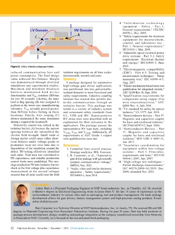
        Figure 5: Critical internal package geometries.                            2012.
                                                                                 7.  “Electromagnetic compatibility
        reduced com munication loss and    isolation requirements on all time scales:   (EMC) - Part 4-5: Testing and
        power consumption. The final design   microseconds, seconds and years.     measurement techniques - Surge
        value achieved this balance. Margin   Summary                              immunity test,” IEC 61000-4-5,
        was demonstrated through electrical   A package designed for automotive    Aug. 2017.
        simulations and experimental studies.   high-voltage gate driver applications   8.  “Failure mechanism based stress test
        Maximum and minimum thickness      was partitioned into two galvanically-  qualification for integrated circuits,”
        bar r iers mai nt ai ned both device   isolated domains to meet functional and   AEC Q100 Rev. H, Sept. 2014.
        functionality and V ISO  isolation (5kVrms   safety requirements. Inductive coupling   9.  “Qualification requirements for
        for over 60 seconds). Likewise, the inner   between two stacked dies permits die-  components using copper (Cu)
        lead to flag spacing (B) was designed to   to-die communications through an   wire interconnections,” AEC
        perform at the worst-case manufacturing   isolation barrier. This package was   Q006 Rev. A, July 2016.
        tolerance. V ISO  actually passed greater   tested to a variety of industry system   10. “UL standard for safety for optical
        than 8kVrms before failing in these   and component safety standards from   isolators,” UL 1577, Apr. 2014.
        locations. Finally, wire looping (C)   UL, VDE and IEC. Representative   11. “Semiconductor devices – Part 17:
        always maintained the same minimum   HV stress tests were described with an   Magnetic and capacitive coupler
        distance required for location B.  explanation for their relevance to the   for basic and reinforced isolation,”
          Defectivity control was critical in the   application. The package passed the   IEC/PAS 60747-17, Sept. 2020.
        isolation barrier (A) because the narrow   representative HV type tests, including   12. “Semiconductor Devices – Part
        spacing between die intensified the   V IOSM , V ISO , and V IORM . Additionally, all   11: Magnetic and capacitive
        electric field strength. Small voids or   requirements of AEC Grade 1 copper   coupler for basic and reinforced
        foreign matter could cause either short-  wire qualifications were met.    isolation,” DIN VDE V 0884-11,
        term failures under voltage peaks or                                       Jan. 2017.
        premature wear-out over time due to   References                        13. “Insulation  coordination  for
        degradation of the insulation around the   1.  Compiled from several sources:   equipment within low-voltage
        defect. PD testing effectively identified   Strategy analytics, HIS, Evercore.  systems – Part 1: Principles,
        such units. Void area was correlated to   2.  B. Carpenter, et al., “Automotive   requirements and tests,” IEC/CEI
        PD capacitance, and suitable production   gate driver package with galvanically   60664-1:2007, Apr. 2007.
        control limits were established. The two-   isolated communication linkage,”   14. “High-voltage test techniques –
        stage production PD test (isolation barrier   SMTAI, Nov. 2021.            Partial discharge measurements,”
        check at the first voltage plus capacitance   3.  “Audio, video and similar electronic   IEC 60270:2000+A1:2015: Dec.
        measurement at the second voltage)      apparatus – Safety requirements,”   2000, amended Nov. 2015.
        ensured that all units could meet the field   IEC60065-1, June 2014.


                       Biographies
                         Ankur Shah is a Principal Packaging Engineer at NXP Semiconductors, Inc., in Chandler, AZ. He received
                       a Master’s degree in Electrical Engineering from Arizona State U. He has 14 years of experience in the
                       semiconductor industry in various roles such as packaging, test and product management. He leads package
                       development efforts for gate drivers, battery management system and high-precision analog products. Email:
                       ankur.shah@nxp.com

                         Burt Carpenter is a Technical Director at NXP Semiconductors, Inc., in Austin, TX. He received BS and MS
          degrees in Materials Engineering from Rensselaer Polytechnic Institute. During the past 29 years, Burt has held positions in
          package process development, design, modeling and package integration as the company transitioned ownership from Motorola
          to Freescale to NXP. Currently, he is focused on fan-out and panel-level packaging.


        22
        22   Chip Scale Review   November  •  December  •  2023   [ChipScaleReview.com]

