Page 22 - Chip Scale Review_November-December_2023-digital
P. 22
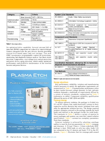
Table 1: Key design criteria.
        for optimized drive capability. Several external bill of
        materials (BOM) components are reduced or removed though
        features integrated into the gate drivers, thereby providing
        system-level board space and cost savings. This new
        GDIC incorporates programmable control for protections,
        monitoring, and diagnostic features such as <1µs short-circuit
        detection, temperature, over-voltage/over-current protection
        and power device aging detection, which enable optimized
        performance and predictive maintenance of the traction
        inverter and power devices.


                                                             Table 2: Applicable standards and description.
                                                             Design objectives
                                                               Key performance, reliability, isolation and manufacturing
                                                             criteria necessary to satisfy the application requirements are
                                                             summarized in Table 1. Communication performance refers
                                                             to data transfer between voltage domains. In fact, galvanic
                                                             isolation demands a multitude of requirements driven by
                                                             a variety of industry standards, summarized in Table 2
                                                             (references in table). Component reliability qualification
                                                             followed the norms of AEC Q100 and Q006.
                                                             Package design
                                                               To achieve galvanic isolation, the package is divided into
                                                             LV and HV regions that could electrically connect to their
                                                             respective system domains but remain insulated from each
                                                             other by appropriate isolation barriers. The design required
                                                             isolation strategies external to the package (outside the mold
                                                             body) and internal to the package (inside the mold body).
                                                             The standards in Table 2 define a variety of metrics to
                                                             ensure packages and systems can meet their stated isolation
                                                             specifications. Table 3 summarizes exemplary parameters
                                                             from these standards.
                                                               External isolation is achieved by selecting a package
                                                             outline to meet the first two parameters in Table 3: creepage
                                                             and clearance. A 32-lead 7.5mm x 11.0mm wide-body SOIC
                                                             package is ideal. With leads on only two sides, leads 1-16
                                                             are connected to the LV domain and leads 17-32 to the HV
                                                             domain. Figure 2 illustrates that the creepage path around

        20
        20   Chip Scale Review   November  •  December  •  2023   [ChipScaleReview.com]

