Page 23 - Chip Scale Review_November-December_2023-digital
P. 23
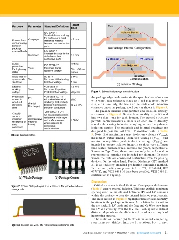
Figure 4: Schematic of package internal structure.
                                                             the package edge could maintain the specification value even
                                                             with worst-case tolerance stack-up (lead placement, body
                                                             size, etc.). Similarly, the heels of the leads could maintain
                                                             clearance under the package mold body as shown in Figure 3.
                                                               The package internal configuration and isolation strategy
                                                             are shown in Figure 4. Device functionality is partitioned
                                                             into two dies—one for each domain. The stacked structure
                                                             permits communication elements on each die to directly
                                                             transfer data using inductive coupling across the galvanic
                                                             isolation barrier. The materials and internal spacings are
                                                             designed to pass the last five HV isolation tests in Table
        Table 3: Isolation metrics.                          3. Note that maximum surge isolation voltage (V IOSM ),
                                                             maximum withstanding isolation voltage (V ISO ), and
                                                             maximum repetitive peak isolation voltage (V IORM ) are
                                                             intended to ensure isolation integrity on three very different
                                                             time scales: microseconds, seconds and years, respectively.
                                                             Known as Type Tests, these three can only be performed on
                                                             representative samples not intended for shipment. In other
                                                             words, the tests are considered destructive even for passing
                                                             devices. On the other hand, Partial Discharge (PD) method
                                                             B1 is an industry standard production screening method.
                                                             Furthermore, safety compliance to UL 1577, IEC 60664, IEC
                                                             6074717, and VDE 0884-10 have been certified. VDE 0884-11
                                                             certification is ongoing.
                                                             Discussion
        Figure 2: 32-lead SOIC package (7.5mm x 11.0mm). The yellow line indicates   Critical distances in the definitions of creepage and clearance
        creepage path.                                       (Table 3) ensure external isolation. While not explicit, minimum
                                                             spacing must be maintained between HV and LV domains
                                                             within the package to pass the internal isolation requirements.
                                                             The cross section in Figure 5 highlights three critical geometry
                                                             locations in the package as follows: A: Isolation barrier within
                                                             the die stack; B: LV leads and die flag; and C: Wire loop from
                                                             the LV die crossing over the HV die. Each specific critical
                                                             distance depends on the dielectric breakdown strength of
                                                             intervening material.
                                                               The isolation barrier (A) thickness balanced competing
                                                             requirements: thicker improved isolation, but thinner
        Figure 3: Package side view.  The red line indicates clearance path.

                                                                                                             21
                                                       Chip Scale Review   November  •  December  •  2023   [ChipScaleReview.com]  21

